RX23W Group 44. 12-Bit A/D Converter (S12ADE) register as 2-bit extended data of the conversion accuracy bits: when the conversion count is set to 16 times, the value added by the A/D conversion result is retained in the ADBUFn register as 4-bit extended data of the conversion accuracy bits. Even if A/D-converted value addition mode is selected, the extended A/D-converted value is stored in the ADBUFn register according to the settings of the A/D data register format select bits. 44.2.
RX23W Group 44.2.38 44. 12-Bit A/D Converter (S12ADE) A/D Data Storage Buffer Pointer Register (ADBUFPTR) Address(es): S12AD.ADBUFPTR 0008 90D2h Value after reset: b7 b6 b5 b4 — — — PTROV F 0 0 0 0 b3 b2 b1 b0 BUFPTR[3:0] 0 0 0 0 Bit Symbol Bit Name Description R/W b3 to b0 BUFPTR[3:0] Data Storage Buffer Pointer These bits indicate the number of data storage buffer to which the next A/D conversion data is transferred.
RX23W Group 44.3 44.3.1 44. 12-Bit A/D Converter (S12ADE) Operation Scanning Operation In scanning, A/D conversion is performed sequentially on the analog inputs of the specified channels. A scan conversion is performed in three operating modes: single scan mode, continuous scan mode, and group scan mode. Also, conversion modes are divided into high-speed conversion mode and normal conversion mode. In single scan mode, one or more specified channels are scanned once.
RX23W Group 44.3.2 44.3.2.1 44. 12-Bit A/D Converter (S12ADE) Single Scan Mode Basic Operation In basic operation of single scan mode, A/D conversion is performed once on the analog input of the specified channels as below. (1) When the ADCSR.ADST bit is set to 1 (A/D conversion start) by software, synchronous trigger, or asynchronous trigger input, A/D conversion is performed for ANn channels selected by the ADANSA0 and ADANSA1 registers, starting from the channel with the smallest number n.
RX23W Group 44.3.2.2 44. 12-Bit A/D Converter (S12ADE) Channel Selection and Self-Diagnosis When channels and self-diagnosis are selected, A/D conversion is performed once for the reference voltage VREFH0 supplied to the 12-bit A/D converter as below. After that, A/D conversion is performed only once on the analog input of the selected channels. (1) A/D conversion for self-diagnosis is started when the ADCSR.
RX23W Group 44.3.2.3 44. 12-Bit A/D Converter (S12ADE) A/D Conversion of Temperature Sensor Output/Internal Reference Voltage A/D conversion of the temperature sensor output and internal reference voltage is performed in single scan mode as below. All channels should be deselected (by setting the ADANSA0 and ADANSA01 register bits to all 0 and the ADCSR.DBLE bit to 0).
RX23W Group 44.3.2.4 44. 12-Bit A/D Converter (S12ADE) A/D Conversion in Double Trigger Mode In single scan mode with double trigger mode, single scan operation started by synchronous trigger is performed twice as below. Self-diagnosis should be deselected, and the temperature sensor output A/D conversion select bit (ADEXICR.TSSA) and the internal reference voltage A/D conversion select bit (ADEXICR.OCSA) should be set to 0.
RX23W Group 44.3.3 44. 12-Bit A/D Converter (S12ADE) Continuous Scan Mode 44.3.3.1 Basic Operation In basic operation of continuous scan mode, A/D conversion is performed repeatedly on the analog input of the specified channels as below. In continuous scan mode, the temperature sensor output A/D conversion select bit (ADEXICR.TSSA) and the internal reference voltage A/D conversion select bit (ADEXICR.OCSA) should be set to 0 (deselected). (1) When the ADCSR.
RX23W Group 44.3.3.2 44. 12-Bit A/D Converter (S12ADE) Channel Selection and Self-Diagnosis When channels and self-diagnosis are selected at the same time, A/D conversion is first performed for the reference voltage VREFH0 supplied to the 12-bit A/D converter, and then A/D conversion is performed on the analog input of the selected channels, which sequence is repeated as below. In continuous scan mode, the temperature sensor output A/D conversion select bit (ADEXICR.
RX23W Group 44.3.4 44.3.4.1 44. 12-Bit A/D Converter (S12ADE) Group Scan Mode Basic Operation In basic operation of group scan mode, A/D conversion is performed once on the analog inputs of all the specified channels in group A and group B after scanning is started by a synchronous trigger as below. Scan operation of each group is similar to the scan operation in single scan mode. The synchronous triggers of group A and B can be selected using the TRSA[5:0] and TRSB[5:0] bits in ADSTRGR, respectively.
RX23W Group 44.3.4.2 44. 12-Bit A/D Converter (S12ADE) A/D Conversion in Double Trigger Mode When double trigger mode is selected in group scan mode, two rounds of single scan operation started by a synchronous trigger are performed as a sequence for group A. For group B, single scan operation started by a synchronous trigger is performed once. In group scan mode, the synchronous triggers of group A and B can be selected using the TRSA[5:0] and TRSB[5:0] bits in ADSTRGR, respectively.
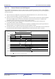
RX23W Group 44.3.4.3 44. 12-Bit A/D Converter (S12ADE) Operation under Group-A Priority Control Setting the PGS bit in the A/D group scan priority control register (ADGSPCR) to 1 in group scan mode makes operation proceed under group-A priority control. When setting the PGS bit in the ADGSPCR register to 1, follow the procedure described in Figure 44.13. If the procedure is not followed, A/D conversion operation and stored data are not guaranteed.
RX23W Group 44. 12-Bit A/D Converter (S12ADE) Start Are the ADCSR.ADCS[1:0] bits set to 01b (group scan mode)? No To disable trigger input, set the ADSTRGR.TRSA[5:0] bits to 3Fh Yes Are the ADCSR.ADCS[1:0] bits set to 10b (continuous scan mode)? No Yes Set the ADCSR.ADST bit to 0 (A/D conversion stop state) To disable trigger input, set the ADSTRGR register to 3F3Fh (set the TRSA[5:0] bits and the TRSB[5:0] bits to 3Fh and 3Fh, respectively) To disable trigger input, set the ADSTRGR.
RX23W Group Table 44.9 44. 12-Bit A/D Converter (S12ADE) Control of A/D Conversion Operations According to the Settings of the ADGSPCR.GBRSCN Bit A/D Conversion Operation Trigger Input ADGSPCR.GBRSCN = 0 ADGSPCR.GBRSCN = 1 When A/D conversion for group A is in progress Input of trigger for group A Trigger input is ineffective. Trigger input is ineffective. Input of trigger for group B Trigger input is ineffective.
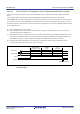
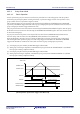
RX23W Group 44. 12-Bit A/D Converter (S12ADE) A/D conversion on group A under group-A priority control First A/D conversion on group B (Group B is activated by a group B trigger.) Second A/D conversion on group B (Group B is automatically activated for rescanning.
RX23W Group 44. 12-Bit A/D Converter (S12ADE) (7) On completion of A/D conversion on the group A, rescanning operation on group B sets the ADCSR.ADST bit to 1 automatically if the setting of the ADGSPCR.GBRSCN bit is 1 (rescanning operation enabled). After that, A/D conversion for the ANn group B channels selected in the ADANSB0 and ADANSB1 registers starts again in order from the channel with the lowest number n.
RX23W Group 44. 12-Bit A/D Converter (S12ADE) The following is an example of a rescanning operation in which a group B trigger is input during A/D conversion on group A. In this example, channels 1 to 3 are selected for group A and channel 0 is selected for group B when operation on group A is given priority (ADGSPCR.GBRSCN = 1, ADGSPCR.GBRP = 0). (1) When input of a trigger for group A sets the ADCSR.
RX23W Group 44. 12-Bit A/D Converter (S12ADE) A/D conversion on group B (Group B is activated by rescanning.) First A/D conversion on group A (Group A is activated by a group A trigger.
RX23W Group 44. 12-Bit A/D Converter (S12ADE) The following is an example of operation under group-A priority control in which channel 0 is selected for group A and channels 1 to 3 are selected for group B (ADGSPCR.GBRSCN = 0, ADGSPCR.GBRP = 0). (1) When input of a trigger for group B sets the ADCSR.ADST bit to 1 (A/D conversion start), conversion for the ANn channels selected in the ADANSB0 and ADANSB1 registers, starting from the channel with the smallest number n.
RX23W Group 44. 12-Bit A/D Converter (S12ADE) The following is an example of operation under group-A priority control in which channel 0 is selected for group A and channels 1 to 3 are selected for group B (ADGSPCR.GBRP = 1). (1) The ADCSR.ADST bit is set to 1 (A/D conversion start) when ADGSPCR.GBRP is set to 1, and conversion for the ANn channels selected in the ADANSB0 and ADANSB1 registers, starting from the channel with the smallest number n.
RX23W Group 44.3.5 44.3.5.1 44. 12-Bit A/D Converter (S12ADE) Compare Function (Window A, Window B) Compare Function Window A/B The compare function compares the reference value set in the register with the A/D conversion result. The reference value can be set for window A and window B independently. When the compare function is in use, the self-diagnosis function and double trigger mode cannot be used.
RX23W Group 44.
RX23W Group 44.3.5.2 44. 12-Bit A/D Converter (S12ADE) ELC Output of Compare Function The ELC output of the compare function is used to specify the high-side reference value and the low-side reference value for window A and window B respectively, and to compare the A/D converted value of the selected channel with the high/ low-side reference value.
RX23W Group 44.
RX23W Group 44.3.5.3 44. 12-Bit A/D Converter (S12ADE) Using Data Buffers This S12ADE is provided with a ring buffer function consisting of 16 A/D data buffers. This function sequentially stores A/D conversion results other than self-diagnosis result (including addition/average results) in data buffers (ADBUFn, n = 0 to 15) when the compare function is used.
RX23W Group 44.3.5.4 44. 12-Bit A/D Converter (S12ADE) Restrictions for Compare Function The following restrictions are provided for the compare function. 1. The compare function must not be used together the self-diagnosis function or double trigger mode. (The compare function is not available for the ADRD register and the ADDBLDR register.) 2. Specify single scan mode when using match/mismatch event outputs. 3.
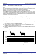
RX23W Group Table 44.10 44. 12-Bit A/D Converter (S12ADE) Times for Conversion during Scanning (in Numbers of Cycles of ADCLK and PCLK) Type/Conditions Item Scan start processing time*1, *2 Symbol Synchronous Trigger *5 Asynchronous Trigger tD 3 PCLK + 6 ADCLK — — A/D conversion on group A under group-A priority control. Group B is to be stopped. (Group A is activated after group B is stopped due to an A/D conversion source of group A.) Group B is not to be stopped.
RX23W Group 44. 12-Bit A/D Converter (S12ADE) tSCAN Asynchronous trigger (External trigger) tD tDIAG tCONV Waiting DIAG conversion A/D conversion tED ADST bit A/D converter Figure 44.23 44.3.7 End processing Scan Conversion Timing (Activated by Asynchronous Trigger) Usage Example of A/D Data Register Automatic Clearing Function Setting the ADCER.
RX23W Group 44.3.9 44. 12-Bit A/D Converter (S12ADE) Disconnection Detection Assist Function This converter incorporates the function to fix the charge for sampling capacitance to the specified state (reference voltage selected by the A/D high-potential/low-potential reference voltage control register) before start of A/D conversion. This function enables disconnection detection in wiring of analog inputs. Figure 44.
RX23W Group 44. 12-Bit A/D Converter (S12ADE) OFF ON Analog input ANn Disconnection R = 1 MΩ Precharge control signal Discharge control signal Discharge Sampling capacitance VREFL0 or AVSS0 Example of the external circuit*1 Note 1. The converted result should be used after fully evaluated because the result data when disconnection occurs varies depending on the external circuit. Figure 44.26 Example of Disconnection Detection When Discharge is Selected R01UH0823EJ0110 Rev.1.
RX23W Group 44.3.10 44. 12-Bit A/D Converter (S12ADE) Starting A/D Conversion with Asynchronous Trigger The A/D conversion can be started by the input of an asynchronous trigger. To start up the A/D converter by an asynchronous trigger, the A/D conversion start trigger select bits (ADSTRGR.TRSA[5:0]) should be set to 000000b, and a high-level signal should be input to the asynchronous trigger (ADTRG0# pin). Then, the ADCSR.TRGE and ADCSR.EXTRG bits should be set to 1. Figure 44.
RX23W Group 44.5 44.5.1 44. 12-Bit A/D Converter (S12ADE) Event Link Function Event Output to the ELC The ELC uses the S12ADI0 interrupt request signal as an event signal (S12ADELC), enabling link operation for the preset module. An event signal is generated under the conditions set by the event link control bits (ADELCCR.ELCC[1:0] bits). The event signal can be output regardless of the setting of the corresponding interrupt request enable bit.
RX23W Group 44.7 44. 12-Bit A/D Converter (S12ADE) Allowable Impedance of Signal Source To achieve high-speed conversion of 0.83 µs, the analog input pins of this MCU are designed so that the conversion accuracy is guaranteed if the impedance of the input signal source is 0.5 kΩ or less. If an external capacitor of large capacitance is attached in the application in which only a single pin input is converted in single scan mode, the only load on input is virtually 2.
RX23W Group 44.8 44. 12-Bit A/D Converter (S12ADE) Usage Notes 44.8.1 Notes on Reading Data Registers Read the A/D data registers, A/D data duplication register, A/D data duplication register A, A/D data duplication register B, A/D temperature sensor data register, A/D internal reference voltage data register, and A/D self-diagnosis data register in word units.
RX23W Group 44.8.3 44. 12-Bit A/D Converter (S12ADE) A/D Conversion Restarting Timing and Termination Timing It takes a maximum of six ADCLK cycles for the idle analog unit of the 12-bit A/D converter to be restarted by setting the ADCSR.ADST bit to 1. It takes a maximum of three ADCLK cycles for the operating analog unit of the 12-bit A/D converter to be terminated by setting the ADCSR.ADST bit to 0. 44.8.
RX23W Group 44.8.10 44. 12-Bit A/D Converter (S12ADE) ADHSC Bit Rewriting Procedure Before rewriting the A/D conversion select bit (ADCSR.ADHSC) from 0 to 1 or from 1 to 0, the 12-bit A/D converter must be in the standby state. Carry out steps 1 to 3 below to modify the ADCSR.ADHSC bit. After the sleep bit (ADHVREFCNT.ADSLP) is cleared to 0, wait for at least 1 µs and then start A/D conversion. ADHSC Bit Rewriting Procedure: 1. Set the sleep bit (ADHVREFCNT.ADSLP) to 1. 2. Wait for at least 0.
RX23W Group 44.8.11 44. 12-Bit A/D Converter (S12ADE) Voltage Range of Analog Power Supply Pins If this MCU is used with the voltages outside the following ranges, the reliability of the MCU may be affected. • Analog input voltage range Voltage applied to analog input pins ANn: AVSS0 ≤ VAN ≤ AVCC0 Reference voltage range applied to pins VREFH0 and VREFL0: VREFH0 ≤ AVCC0, VREFL0 = AVSS0 Conversion will not succeed if the voltage applied to analog input pins ANn is greater than VREFH0 (see Figure 44.30).
RX23W Group 44.8.12 44. 12-Bit A/D Converter (S12ADE) Notes on Board Design The board should be designed so that digital circuits and analog circuits are separated from each other as far as possible. In addition, digital circuit signal lines and analog circuit signal lines should not intersect or placed near each other. If these rules are not followed, noise will be produced on analog signals and A/D conversion accuracy will be affected.
RX23W Group 45. 12-Bit D/A Converter (R12DAA) 45. 12-Bit D/A Converter (R12DAA) 45.1 Overview This MCU includes two channels of 12-bit D/A converter. Table 45.1 lists the specifications of the 12-bit D/A converter and Figure 45.1 shows a block diagram of the 12-bit D/A converter. Table 45.
RX23W Group 45. 12-Bit D/A Converter (R12DAA) Table 45.2 lists the pin configuration of the 12-bit D/A converter. Table 45.2 Pin Configuration of 12-Bit D/A Converter Pin Name I/O Function AVCC0 Input Analog voltage supply pin for the 12-bit A/D converter and 12-bit D/A converter. Connect this pin to VCC when not using the 12-bit A/D converter and 12-bit D/A converter. AVSS0 Input Analog ground pin for the 12-bit A/D converter and 12-bit D/A converter.
RX23W Group 45.2.2 45. 12-Bit D/A Converter (R12DAA) D/A Control Register (DACR) Address(es): DA.DACR 0008 8044h b7 b6 DAOE1 DAOE0 0 Value after reset: 0 b5 b4 b3 b2 b1 b0 — — — — — — 0 1 1 1 1 1 Bit Symbol Bit Name Description R/W b4 to b0 — Reserved These bits are read as 1. The write value should be 1. R/W b5 — Reserved This bit is read as 0. The write value should be 0. R b6 DAOE0 D/A Output Enable 0 0: Analog output of channel 0 (DA0) is disabled.
RX23W Group 45.2.4 45. 12-Bit D/A Converter (R12DAA) D/A A/D Synchronous Start Control Register (DAADSCR) Address(es): DA.DAADSCR 0008 8046h b7 b6 b5 b4 b3 b2 b1 b0 DAADS T — — — — — — — 0 0 0 0 0 0 0 0 Value after reset: Bit Symbol Bit Name Description R/W b6 to b0 — Reserved These bits are read as 0. The write value should be 0. R/W b7 DAADST D/A A/D Synchronous Conversion 0: 12-bit D/A converter operation does not synchronize with 12-bit A/D converter operation.
RX23W Group 45.2.5 45. 12-Bit D/A Converter (R12DAA) D/A VREF Control Register (DAVREFCR) Address(es): DA.DAVREFCR 0008 8047h Value after reset: b7 b6 b5 b4 b3 — — — — — 0 0 0 0 0 b2 b1 b0 REF[2:0] 0 0 0 Bit Symbol Bit Name Description R/W b2 to b0 REF[2:0] D/A Reference Voltage Select b2 R/W b7 to b3 — Reserved b0 0 0 0: Not selected 0 0 1: AVCC0/AVSS0 0 1 1: Internal reference voltage/AVSS0 Settings other than above are prohibited. These bits are read as 0.
RX23W Group 45.3 45. 12-Bit D/A Converter (R12DAA) Operation The 12-bit D/A converter includes D/A conversion circuits for two channels, each of which can operate independently. When the DACR.DAOEm bit (m = 0, 1) is set to 1, D/A converter is enabled and the conversion result is output. An operation example of D/A conversion on channel 0 is shown below. Figure 45.2 shows the timing of this operation. (1) Set the data for D/A conversion in the DADPR.DPSEL bit and the DADR0 register. (2) Set the DACR.
RX23W Group 45.3.1 45. 12-Bit D/A Converter (R12DAA) Measure against Interference between D/A and A/D Conversion When D/A conversion starts, an inrush current occurs to the 12-bit D/A converter. Since the same analog power supply is shared by the 12-bit D/A converter and 12-bit A/D converter, the inrush current may interfere with the proper operation of the 12-bit A/D converter. With the DAADSCR.
RX23W Group 45. 12-Bit D/A Converter (R12DAA) When ADCLK is faster than PCLKB, the 12-bit D/A converter may not be able to capture a 12-bit A/D converter synchronous D/A conversion enable signal for one ADCLK cycle which is output between A/D conversion 1 and A/D conversion 2. Figure 45.4 shows example when the 12-bit D/A converter cannot capture the 12-bit A/D converter synchronous D/A conversion enable signal. In this case, the DA0 output is held at the level of the post-D/A conversion value A.
RX23W Group 45.3.2 45. 12-Bit D/A Converter (R12DAA) Notes on Using the Internal Reference Voltage as the Reference Voltage When setting the DAVREFCR.REF[2:0] bits to 011b to use the internal reference voltage/AVSS0 as the reference voltage, the VREF path needs to be discharged before selecting the voltage. The following shows the discharging procedure. (1) (2) (3) (4) (5) Write 000b to the REF[2:0] bits. Set the DADR0 register to 0000h and the DADR1 register to 0000h.
RX23W Group 45.4 45. 12-Bit D/A Converter (R12DAA) Event Link Operation Setting Procedure The event link operation procedure is described below. (1) Set the DADPR.DPSEL bit and set the data for D/A conversion in the DADR0 register. (2) Set the bit value of the ELSR16 setting event signal to link the ELSR16 register of the ELC. (3) Set the ELCR.ELCON bit to 1. This procedure enables event link operation for all modules with the event link function selected.
RX23W Group 45.6 45.6.1 45. 12-Bit D/A Converter (R12DAA) Usage Notes Module Stop Function Setting Operation of the 12-bit D/A converter can be disabled or enabled using the module stop control register. The initial setting is for operation of the 12-bit D/A converter to be stopped. Register access is enabled by releasing the module stop state. For details, refer to section 11, Low Power Consumption. 45.6.
RX23W Group 46. Temperature Sensor (TEMPSA) 46. Temperature Sensor (TEMPSA) 46.1 Overview This MCU includes a temperature sensor. The temperature sensor outputs a voltage which varies with the temperature. The user can obtain the temperature surrounding the MCU using the 12-bit A/D converter to convert the voltage output from the temperature sensor into a digital value. Table 46.1 lists the specifications of the temperature sensor. Figure 46.
RX23W Group 46.2 46. Temperature Sensor (TEMPSA) Register Descriptions 46.2.1 Temperature Sensor Calibration Data Register (TSCDRH, TSCDRL) Address(es): TEMPSCONST.TSCDRL 007F C0ACh b7 b6 b5 b4 b3 b2 b1 b0 b1 b0 Unique value for each chip Value after reset: Address(es): TEMPSCONST.TSCDRH 007F C0ADh b7 b6 Value after reset: b5 b4 b3 b2 Unique value for each chip The TSCDRH and TSCDRL registers store temperature sensor calibration data measured for each chip at factory shipment.
RX23W Group 46.3 46. Temperature Sensor (TEMPSA) Using the Temperature Sensor The temperature sensor outputs a voltage which varies with the temperature. The user can obtain the temperature surrounding the MCU using the 12-bit A/D converter to convert this voltage into a digital value. 46.3.1 Before Using the Temperature Sensor Perform a calibration of the temperature sensor as shown below.
RX23W Group 46. Temperature Sensor (TEMPSA) T: Measured temperature (°C) Vs: Voltage output by the temperature sensor when the temperature is measured (V) V1: Voltage output by the temperature sensor when Ta = Tj = 88°C and AVCC0 = VREFH0 = 3.3 V (V) Slope: Temperature gradient listed in Table 51.56 ÷ 1000 (V/°C) Error in the measured temperature (the range of variation is 3σ) is shown in Figure 46.2. ±12.0 ±10.0 Error (3σ) [°C] ±8.0 ±6.0 ±4.0 ±2.0 ±0.
RX23W Group 47. 47. Comparator B (CMPBa) Comparator B (CMPBa) Comparator B compares a reference input voltage and an analog input voltage. comparator B2 and comparator B3 operate independently. In this section, “PCLK” is used to refer to PCLKB. 47.1 Overview The comparison result of the reference input voltage and analog input voltage can be read by software. The comparison result can also be output externally.
RX23W Group 47.
RX23W Group 47.
RX23W Group 47.2 47. Comparator B (CMPBa) Register Descriptions 47.2.1 Comparator B1 Control Register 1 (CPB1CNT1) Address: 0008 C5A0h Value after reset: b7 b6 b5 b4 b3 b2 b1 b0 — — — CPB3I NI — — — CPB2I NI 0 0 0 0 0 0 0 0 Bit Symbol Bit Name Description R/W b0 CPB2INI Comparator B2 Power Enable 0: Disabled 1: Enabled (comparator powered on) R/W b3 to b1 — Reserved These bits are read as 0. The write value should be 0.
RX23W Group 47.2.3 47. Comparator B (CMPBa) Comparator B1 Flag Register (CPB1FLG) Address: 0008 C5A2h b7 b6 b5 b4 b3 b2 b1 b0 CPB3O UT — — — CPB2O UT — — — 0 0 0 0 0 0 0 0 Value after reset: Bit Symbol Bit Name Description R/W b2 to b0 — Reserved These bits are read as 0. The write value should be 0.
RX23W Group 47.2.4 47.
RX23W Group 47.2.5 47. Comparator B (CMPBa) Comparator B1 Filter Select Register (CPB1F) Address: 0008 C5A4h b7 Value after reset: b6 b5 b4 CPB3F[1:0] — CPB3F EN 0 0 0 0 b3 b2 b1 b0 CPB2F[1:0] — CPB2F EN 0 0 0 0 Bit Symbol Bit Name Description R/W b0 CPB2FEN Comparator B2 Filter Enable/Disable Select*1 0: Filter is disabled. 1: Filter is enabled. R/W b1 — Reserved This bit is read as 0. The write value should be 0.
RX23W Group 47.2.7 47.
RX23W Group 47.2.8 47.
RX23W Group 47.3 47. Comparator B (CMPBa) Operation Comparator B2 and comparator B3 operate independently, and their operations are the same. Operation is not guaranteed when the values of registers are changed during comparator operation. Table 47.3 shows the procedure of setting comparator B associated registers when the window function is disabled. Table 47.4 shows the procedure of setting comparator B associated registers when the window function is enabled. Table 47.3 Step No.
RX23W Group Table 47.4 Step No. 47. Comparator B (CMPBa) Procedure for Setting Registers Associated with Comparator B When Window Function is Enabled (n = 2, 3) Register Bit 1 PijPFS of the port to which the CMPBn pin is assigned ASEL 2 CPB1MD CPBSPDMD 3 CPB1CNT1 CPBnINI 4 CPB1F Select whether to enable or disable the filter and select the sampling clock. 5 CPB1CNT2 CPBnWCP 6 Waiting for the comparator stabilization time (min.
RX23W Group 47. Comparator B (CMPBa) Figure 47.3 shows an operating example of comparator Bn (n = 2, 3) when window function is disabled. The reference input voltage (CVREFB2/CVREFB3 or internal reference voltage) and the analog input voltage are compared. If the analog input voltage is higher than the reference input voltage, the CPB1FLG.CPBnOUT bit is set to 1. If the analog input voltage is lower than the reference input voltage, the CPBnOUT bit is set to 0.
RX23W Group 47. Comparator B (CMPBa) Figure 47.4 shows an operation example of comparator Bn (n = 2, 3) when the window function is enabled. The internal reference voltage (VRFH/VRFL) for the window function and the analog input voltage are compared. The CPBnOUT bit is set to 1 when VRFL < the analog input voltage < VRFH, and the CPBnOUT bit is set to 0 when the analog input voltage < VRFL, or VRFH < the analog input voltage. To use the comparator Bn interrupt, set the CPB1INT.
RX23W Group 47.3.1 47. Comparator B (CMPBa) Comparator Bn Digital Filter (n = 2, 3) The sampling clock can be selected by the CPB1F.CPBnF[1:0] bits. The CPBnOUT signal (internal signal) output from comparator Bn is sampled at every sampling clock cycle. At the next clock timing after the level matches three times, the IR104.IR flag (when comparator B2 selected) or IR105.IR flag (when comparator B3 selected) is set to 1 (interrupt requested). Figure 47.
RX23W Group 47.3.2 47. Comparator B (CMPBa) Comparator Bn Output Function (n = 2, 3) The comparison result from comparator B can be output to external pins. The CPB1OCR.CPBnOP and CPB1OCR.CPBnOE bits can be used to set the output polarity (non-inverted output or inverted output) and output enabled or disabled. For the register settings and corresponding comparator output, refer to section 47.2.8, Comparator B1 Output Control Register (CPB1OCR).
RX23W Group 47.4 47. Comparator B (CMPBa) Comparator B2 and Comparator B3 Interrupts Comparator B generates two interrupt requests from sources, comparator B2 and . The comparator Bn interrupt (n = 2, 3) uses the IR104.IR flag, IR105.IR flag, IPR104.IPR[3:0] bits, IPR105.IPR[3:0] bits, and the respective single interrupt vector. To use the comparator Bn interrupt, set the CPB1INT.CPBnINTEN bit to 1 (interrupt enabled).
RX23W Group 48. Data Operation Circuit (DOC) 48. Data Operation Circuit (DOC) 48.1 Overview The data operation circuit (DOC) is used to compare, add, or subtract 16-bit values. Table 48.1 lists the specifications of the DOC and Figure 48.1 is a block diagram of the DOC. An interrupt can be generated if the result of 16-bit comparison meets one of the set interrupt conditions. Table 48.
RX23W Group 48.2 48. Data Operation Circuit (DOC) Register Descriptions 48.2.1 DOC Control Register (DOCR) Address(es): DOC.DOCR 0008 B080h b7 — Value after reset: b6 b5 b4 DOPCF DOPCF DOPCI CL E 0 0 0 0 b3 b2 — DCSEL 0 0 b1 b0 OMS[1:0] 0 0 Bit Symbol Bit Name Description R/W b1, b0 OMS[1:0] Operating Mode Select b1 b0 R/W b2 DCSEL Detection Condition Select *1 0: ‘Not equal to’ is to be detected. 1: ‘Equal to’ is to be detected.
RX23W Group 48. Data Operation Circuit (DOC) DOPCFCL Bit (Data Operation Result Clear) Writing 1 to this bit clears the DOPCF flag. This bit is read as 0. 48.2.2 DOC Data Input Register (DODIR) Address(es): DOC.DODIR 0008 B082h Value after reset: b15 b14 b13 b12 b11 b10 b9 b8 b7 b6 b5 b4 b3 b2 b1 b0 0 0 0 0 0 0 0 0 0 0 0 0 0 0 0 0 The DODIR register is a readable and writable register that holds values for use in operations. 48.2.
RX23W Group 48.3 48. Data Operation Circuit (DOC) Operation 48.3.1 Data Comparison Mode Figure 48.2 shows an example of the steps involved in data comparison mode operation by the DOC. An example of operation when DCSEL is set to 0 (‘not equal to’ is to be detected as the result of data comparison) is shown below. (1) (2) (3) (4) (5) Writing 00b to the DOCR.OMS[1:0] bits places the DOC in the data comparison mode. Specify the standard value for comparison in the DODSR register.
RX23W Group 48.3.2 48. Data Operation Circuit (DOC) Data Addition Mode Figure 48.3 shows an example of the steps involved in data addition mode operation by the DOC. (1) (2) (3) (4) (5) Writing 01b to the DOCR.OMS[1:0] bits selects data addition mode. Set the initial value in the DODSR register. Write the value for addition in the DODIR register. The result of the operation is stored in DODSR. Write all values for use in addition to the DODIR register.
RX23W Group 48.3.3 48. Data Operation Circuit (DOC) Data Subtraction Mode Figure 48.4 shows an example of the steps involved in data subtraction mode operation by the DOC. (1) (2) (3) (4) (5) Writing 10b to the DOCR.OMS[1:0] bits selects data subtraction mode. Set the initial value in the DODSR register. Write the value for subtraction in the DODIR register. The result of the operation is stored in DODSR. Write all values for use in subtraction to the DODIR register.
RX23W Group 48.5 48. Data Operation Circuit (DOC) Event Link Output The DOC outputs event signals for the event link controller (ELC) under the following conditions, and these can be used to initiate operations by other modules selected in advance. • The result of data comparison meets the detection condition. • The result of data addition is greater than FFFFh. • The result of data subtraction is less than 0000h. 48.5.
RX23W Group 49. 49. RAM RAM This MCU has an on-chip high-speed static RAM. 49.1 Overview Table 49.1 lists the specifications of the RAM. Table 49.1 Specifications of RAM Item Description Capacity 64 Kbytes (0000 0000h to 0000 FFFFh) Access • Single-cycle access is possible for both reading and writing. • On-chip RAM can be enabled or disabled.*1 Low power consumption function Transitions to the module stopped state are possible. Note 1. Selectable by the RAME bit in SYSCR1.
RX23W Group 50. 50. Flash Memory (FLASH) Flash Memory (FLASH) This MCU has packages with 384 and 512 Kbyte flash memory (ROM) for storing code and 8-Kbyte flash memory (E2 DataFlash) for storing data. In this section, “PCLK” is used to refer to PCLKB. 50.1 Overview Table 50.1 lists the Flash Memory Specifications. Table 50.7 lists the I/O Pins Used in Boot Mode. Table 50.
RX23W Group 50.2 50. Flash Memory (FLASH) ROM Area and Block Configuration The maximum ROM size of this MCU is 512 Kbytes. The ROM area is divided into blocks. A block is 2-Kbyte area. When executing the block erase command, the memory is erased by the block. Figure 50.1 shows the ROM Area and Block Configuration.
RX23W Group 50.3 50. Flash Memory (FLASH) E2 DataFlash Area and Block Configuration The E2 DataFlash is 8 Kbytes in the MCU. The E2 DataFlash is divided into blocks and erased in block units. Figure 50.2 shows the E2 DataFlash Area and Block Configuration.
RX23W Group 50.4 50. Flash Memory (FLASH) Register Descriptions 50.4.1 E2 DataFlash Control Register (DFLCTL) Address(es): FLASH.
RX23W Group 50.4.2 50. Flash Memory (FLASH) Flash P/E Mode Entry Register (FENTRYR) Address(es): FLASH.FENTRYR 007F FFB2h b15 b14 b13 b12 b11 b10 b9 b8 FEKEY[7:0] Value after reset: 0 0 0 0 0 0 0 0 b7 b6 b5 b4 b3 b2 b1 b0 FENTR YD — — — — — — FENTR Y0 0 0 0 0 0 0 0 0 Bit Symbol Bit Name Description R/W b0 FENTRY0 ROM P/E Mode Entry 0 0: ROM is in read mode. 1: ROM can be placed in P/E mode. R/W b6 to b1 — Reserved These bits are read as 0.
RX23W Group 50.4.3 50. Flash Memory (FLASH) Protection Unlock Register (FPR) Address(es): FLASH.FPR 007F C180h Value after reset: b7 b6 b5 b4 b3 b2 b1 b0 x x x x x x x x x: Undefined This write-only register is used to protect the FPMCR register from being rewritten inadvertently when the CPU runs out of control. Writing to the FPMCR register is enabled only when the following procedure is used to access the register.
RX23W Group 50.4.5 50. Flash Memory (FLASH) Flash P/E Mode Control Register (FPMCR) Address(es): FLASH.FPMCR 007F C100h b7 b6 b5 FMS2 LVPE — 0 0 0 Value after reset: b4 b3 FMS1 RPDIS 0 1 b2 b1 b0 — FMS0 — 0 0 0 Bit Symbol Bit Name Description R/W b0 — Reserved This bit is read as 0. The write value should be 0. R/W b1 FMS0 Flash Operating Mode Select 0 FMS2 FMS1 FMS0 R/W b2 — Reserved This bit is read as 0. The write value should be 0.
RX23W Group 50. Flash Memory (FLASH) Wait for ROM mode transition wait time 2 (tMS, refer to section 51, Electrical Characteristics). RPDIS Bit (ROM P/E Disable) This bit is used to disable the execution of ROM programming/erasure with software. LVPE Bit (Low-Voltage P/E Mode Enable) Set this bit to 0 for programming/erasure in high-speed mode, and set this bit to 1 for programming/erasure in middlespeed mode. 50.4.6 Flash Initial Setting Register (FISR) Address(es): FLASH.
RX23W Group Table 50.3 50.
RX23W Group 50.4.7 50. Flash Memory (FLASH) Flash Reset Register (FRESETR) Address(es): FLASH.FRESETR 007F C124h Value after reset: b7 b6 b5 b4 b3 b2 b1 b0 — — — — — — — FRESE T 0 0 0 0 0 0 0 0 Bit Symbol Bit Name Description R/W b0 FRESET Flash Reset 0: Flash control circuit reset is released. 1: Flash control circuit is reset. R/W b7 to b1 — Reserved These bits are read as 0. The write value should be 0.
RX23W Group 50.4.9 50. Flash Memory (FLASH) Flash Control Register (FCR) Address(es): FLASH.FCR 007F C114h b7 b6 b5 b4 OPST STOP — — 0 0 0 0 Value after reset: b3 b2 b1 b0 CMD[3:0] 0 0 0 0 Bit Symbol Bit Name Description R/W b3 to b0 CMD[3:0] Software Command Setting b3 R/W b5, b4 — Reserved These bits are read as 0. The write value should be 0. R/W b6 STOP Forced Processing Stop When this bit is set to 1, the processing being executed can be forcibly stopped.
RX23W Group Table 50.4 50. Flash Memory (FLASH) Setting Address for All-Block Erase Target Memory Size FSARH/FSARL FEARH/FEARL ROM 512 Kbytes FC18 0000h FC1F FFF8h 384 Kbytes FC1A 0000h FC1F FFF8h 8 Kbytes FE00 0000h FE00 1FFFh E2 DataFlash STOP Bit (Forced Processing Stop) This bit is used to forcibly stop the processing (blank check, block erase, or all-block erase) being executed. After setting this bit to 1, wait until the FSTATR1.
RX23W Group 50.4.10 50. Flash Memory (FLASH) Flash Extra Area Control Register (FEXCR) Address(es): FLASH.FEXCR 007F C1DCh b7 b6 b5 b4 b3 OPST — — — — 0 0 0 0 0 Value after reset: b2 b1 b0 CMD[2:0] 0 0 0 Bit Symbol Bit Name Description R/W b2 to b0 CMD[2:0] Software Command Setting b2 R/W b6 to b3 — Reserved These bits are read as 0. The write value should be 0. R/W b7 OPST Processing Start 0: Processing stops. 1: Processing starts.
RX23W Group 50. Flash Memory (FLASH) Writing to the extra area is started by writing 1 to the OPST bit. Do not write to the CMD[2:0] bits while a software command is being executed. 50.4.11 Flash Processing Start Address Register H (FSARH) Address(es): FLASH.
RX23W Group 50.4.13 50. Flash Memory (FLASH) Flash Processing End Address Register H (FEARH) Address(es): FLASH.FEARH 007F C120h b15 Value after reset: 0 b14 0 b13 b12 0 0 b11 0 b10 0 b9 0 b8 b7 b6 b5 — — — — 0 0 0 0 b4 b3 b2 b1 b0 0 0 0 0 0 The FEARH register is used to set the end address of the target processing range in the flash memory when a software command is executed.
RX23W Group 50.4.15 50. Flash Memory (FLASH) Flash Write Buffer Register n (FWBn) (n = 0 to 3) Address(es): FLASH.FWB0 007F C130h, FLASH.FWB1 007F C138h, FLASH.FWB2 007F C140h, FLASH.FWB3 007F C144h Value after reset: b15 b14 b13 b12 b11 b10 b9 b8 b7 b6 b5 b4 b3 b2 b1 b0 0 0 0 0 0 0 0 0 0 0 0 0 0 0 0 0 This register is used to set the data for programming the ROM, E2 DataFlash, or extra area. The data can be written in ROM P/E mode or E2 DataFlash P/E mode.
RX23W Group 50.4.16 50. Flash Memory (FLASH) Flash Status Register 0 (FSTATR0) Address(es): FLASH.FSTATR0 007F C1F0h Value after reset: b7 b6 — — x 0 b5 b4 b3 EILGLE ILGLER BCERR RR R 0 0 b2 — 0 b1 b0 PRGER ERERR R 0 0 0 Bit Symbol Bit Name Description R/W b0 ERERR Erase Error Flag 0: Erasure terminates normally. 1: An error occurs during erasure. R b1 PRGERR Program Error Flag 0: Programming terminates normally. 1: An error occurs during programming.
RX23W Group 50. Flash Memory (FLASH) [Clearing condition] • The next software command is executed. The value read from this flag is undefined when the FCR.STOP bit is set to 1 (processing is forcibly stopped) during blank checking. ILGLERR Flag (Illegal Command Error Flag) This flag indicates the result of executing a software command. [Setting conditions] • Programming/erasure is executed to an area other than the access window range.
RX23W Group 50.4.17 50. Flash Memory (FLASH) Flash Status Register 1 (FSTATR1) Address(es): FLASH.FSTATR1 007F C12Ch b7 b6 EXRDY FRDY Value after reset: 0 0 b5 b4 b3 b2 b1 b0 — — — — — — 0 0 0 1 0 0 Bit Symbol Bit Name Description R/W b1, b0 — Reserved These bits are read as 0. R b2 — Reserved This bit is read as 1. R b5 to b3 — Reserved These bits are read as 0.
RX23W Group 50.4.18 50. Flash Memory (FLASH) Flash Error Address Monitor Register H (FEAMH) Address(es): FLASH.FEAMH 007F C1E8h b15 Value after reset: 0 b14 0 b13 0 b12 0 b11 0 b10 0 b9 0 b8 b7 b6 b5 — — — — 0 0 0 0 b4 b3 b2 b1 b0 0 0 0 0 0 This register is used to check the address where the error has occurred if an error occurs during processing of a software command.
RX23W Group 50.4.20 50. Flash Memory (FLASH) Flash Start-Up Setting Monitor Register (FSCMR) Address(es): FLASH.FSCMR 007F C1C0h Value after reset: b15 b14 b13 b12 b11 b10 b9 b8 b7 b6 b5 b4 b3 b2 b1 b0 — — — — — — — SASMF — — — — — — — — 0 1 1 1 0 1 1 Value set by user*1 0 0 0 0 0 0 0 0 Bit Symbol Bit Name Description R/W b7 to b0 — Reserved These bits are read as 0.
RX23W Group 50.4.22 50. Flash Memory (FLASH) Flash Access Window End Address Monitor Register (FAWEMR) Address(es): FLASH.FAWEMR 007F C1D0h Value after reset: b15 b14 b13 b12 — — — — 0 0 0 0 b11 b10 b9 b8 b7 b6 b5 b4 b3 b2 b1 b0 The value set by the user*1 Note 1. The value of the blank product is 1. It is set to the same value set in bit 11 to bit 0 in the FWB1 register after the access window information program command is executed.
RX23W Group 50.5 50. Flash Memory (FLASH) Start-Up Program Protection When rewriting the start-up program*1 by self-programming, if the rewrite operation is interrupted due to temporary blackout, the start-up program may not be successfully programmed and the user program may not start properly. This problem can be avoided by rewriting the start-up program without erasing the existing start-up program using the start-up program protection.
RX23W Group 50.6 50. Flash Memory (FLASH) Area Protection Area protection enables rewriting only the selected blocks (access window) in the user area and disables rewriting the other blocks during self-programming. The access window cannot be set in the data area. Specify the start address and end address to set the access window. While the access window can be set in boot mode or by self-programming, area protection is enabled only during self-programming in single-chip mode. Figure 50.
RX23W Group 50.7 50. Flash Memory (FLASH) Programming and Erasure The ROM and E2 DataFlash can be programmed and erased by changing the mode of the dedicated sequencer for programming and erasure, and by issuing commands for programming and erasure. The mode transitions and commands required to program or erase the ROM and E2 DataFlash are described below. The descriptions apply in common to boot mode and single-chip mode. 50.7.1 Sequencer Modes The sequencer has four modes.
RX23W Group 50.7.1.2 50. Flash Memory (FLASH) Read Mode Read mode is for high-speed reading of the ROM/E2 DataFlash. Reading from a ROM address for reading can be accomplished in one ICLK clock. (1) ROM/E2 DataFlash Read Mode In this mode, both the ROM and E2 DataFlash are in read mode. The sequencer enters this mode from P/E mode when setting the FPMCR register to 08h, setting the FENTRYR.FENTRYD bit to 0, and setting the FENTRYR.FENTRY0 bit to 0. 50.7.1.
RX23W Group 50.7.2.2 50. Flash Memory (FLASH) Transition from Read Mode to P/E Mode Switching to ROM P/E mode is required before executing a software command for the ROM. Figure 50.8 shows the Procedure for Transition from ROM/E2 DataFlash Read Mode to ROM P/E Mode. Figure 50.9 shows the Procedure for Transition from ROM/E2 DataFlash Read Mode to E2 DataFlash P/E Mode.
RX23W Group 50. Flash Memory (FLASH) Start in ROM/E2 DataFlash read mode FENTRYR register = AA80h Set E2 DataFlash P/E mode Wait for tDSTOP*1 No OPCCR.OPCM[2:0] bits = 000b? Yes High-speed operating mode Set 10h in the FPMCR register FPR register = A5h FPMCR register = 10h FPMCR register = EFh FPMCR register = 10h Middle-speed operating mode Set 50h in the FPMCR register FPR register = A5h FPMCR register = 50h FPMCR register = AFh FPMCR register = 50h Set the FCLK frequency in the FISR.
RX23W Group 50.7.2.3 50. Flash Memory (FLASH) Transition from P/E Mode to Read Mode High-speed reading of the ROM requires switching to ROM/E2 DataFlash read mode. Figure 50.10 shows the Procedure for Transition from ROM P/E Mode to ROM/E2 DataFlash Read Mode. Figure 50.11 shows the Procedure for Transition from E2 DataFlash P/E Mode to ROM/E2 DataFlash Read Mode.
RX23W Group 50. Flash Memory (FLASH) Start in E2 DataFlash P/E mode FPR register = A5h FPMCR register = 08h FPMCR register = F7h FPMCR register = 08h Set 08h in the FPMCR register Wait for tMS*1 FENTRYR register = AA00h FENTRYR register = 0000h? No Yes End in ROM/E2 DataFlash read mode Note 1. tMS: ROM mode transition wait time 2 (Refer to the Electrical Characteristics chapter.) Figure 50.11 Procedure for Transition from E2 DataFlash P/E Mode to ROM/E2 DataFlash Read Mode R01UH0823EJ0110 Rev.1.
RX23W Group 50.7.3 50. Flash Memory (FLASH) Software Commands Software commands consist of commands for programming and erasure and commands for programming start-up program area information and access window information. Table 50.5 lists the software commands for use with the flash memory. Table 50.
RX23W Group 50.7.4 50. Flash Memory (FLASH) Software Command Usage This section describes how to use each software command, using flowcharts. 50.7.4.1 Program Figure 50.12 and Figure 50.13 show the procedure to issue the program command. Start in ROM P/E mode FASR.EXS bit = 0 Set programming address in registers FSARH and FSARL Set programming data in registers FWB0, FWB1, FWB2, and FWB3 FCR register = 81h FSTATR1.FRDY flag = 1? No Yes FCR register = 00h FSTATR1.
RX23W Group 50. Flash Memory (FLASH) Start in E2 DataFlash P/E mode FASR.EXS bit = 0 Set programming address in registers FSARH and FSARL Set programming data in registers FWB0 FCR register = 81h FSTATR1.FRDY flag = 1? No Yes FCR register = 00h FSTATR1.FRDY flag = 0? No Yes FSTATR0.ILGLERR flag = 1 or FSTATR0.PRGERR flag = 1? No Yes Continue E2 DataFlash programming? FRESETR.FRESET bit = 1 Sequencer initialization FRESETR.
RX23W Group 50.7.4.2 50. Flash Memory (FLASH) Block Erase Figure 50.14 and Figure 50.15 show the procedure to issue the block erase command. Start in ROM P/E mode FASR.EXS bit = 0 Set the beginning address of the erasure block in registers FSARH and FSARL Set the last address of the erasure block in registers FEARH and FEARL FCR register = 84h FSTATR1.FRDY flag = 1? No Yes FCR register = 00h FSTATR1.FRDY flag = 0? No Yes FSTATR0.ILGLERR flag = 1 or FSTATR0.
RX23W Group 50. Flash Memory (FLASH) Start in E2 DataFlash P/E mode FASR.EXS bit = 0 Set the beginning address of the erasure block in registers FSARH and FSARL Set the last address of the erasure block in registers FEARH and FEARL FCR register = 84h FSTATR1.FRDY flag = 1? No Yes FCR register = 00h FSTATR1.FRDY flag = 0? No Yes FSTATR0.ILGLERR flag = 1 or FSTATR0.ERERR flag = 1? No Yes Continue E2 DataFlash erasure? FRESETR.FRESET bit = 1 Sequencer initialization FRESETR.
RX23W Group 50.7.4.3 50. Flash Memory (FLASH) All-Block Erase Figure 50.16 and Figure 50.17 show the procedure to issue the all-block erase command. Start in ROM P/E mode FASR.EXS bit = 0 Set the beginning address of the ROM area in registers FSARH and FSARL Set the last address of the ROM area in registers FEARH and FEARL FCR register = 86h FSTATR1.FRDY flag = 1? No Yes FCR register = 00h FSTATR1.FRDY flag = 0? No Yes FSTATR0.ILGLERR flag = 1 or FSTATR0.ERERR flag = 1? No Yes FRESETR.
RX23W Group 50. Flash Memory (FLASH) Start in E2 DataFlash P/E mode FASR.EXS bit = 0 Set the beginning address of the E2 DataFlash area in registers FSARH and FSARL Set the last address of the E2 DataFlash area in registers FEARH and FEARL FCR register = 86h FSTATR1.FRDY flag = 1? No Yes FCR register = 00h FSTATR1.FRDY flag = 0? No Yes FSTATR0.ILGLERR flag = 1 or FSTATR0.ERERR flag = 1? No Yes FRESETR.FRESET bit = 1 Sequencer initialization FRESETR.
RX23W Group 50.7.4.4 50. Flash Memory (FLASH) Blank Check Figure 50.18 and Figure 50.19 show the procedure to issue the blank check command. Start in ROM P/E mode FASR.EXS bit = 0 Set the blank check start address in registers FSARH and FSARL Set the blank check end address in registers FEARH and FEARL FCR register = 83h FSTATR1.FRDY flag = 1? No Yes FCR register = 00h FSTATR1.FRDY flag = 0? No Yes FSTATR0.ILGLERR flag = 1 or FSTATR0.BCERR flag = 1? No Yes FRESETR.
RX23W Group 50. Flash Memory (FLASH) Start in E2 DataFlash P/E mode FASR.EXS bit = 0 Set blank check start address in registers FSARH and FSARL Set blank check end address in registers FEARH and FEARL FCR register = 83h FSTATR1.FRDY flag = 1? No Yes FCR register = 00h FSTATR1.FRDY flag = 0? No Yes FSTATR0.ILGLERR flag = 1 or FSTATR0.BCERR flag = 1? No Yes FRESETR.FRESET bit = 1 Sequencer initialization FRESETR.FRESET bit = 0 End in E2 DataFlash P/E mode Figure 50.
RX23W Group 50.7.4.5 50. Flash Memory (FLASH) Start-Up Area Information Program/Access Window Information Program Figure 50.20 shows the procedure to issue the start-up area information program command and access window information program command. When the sequencer has directly entered ROM/PE mode from E2 DataFlash access disabled mode, set the DFLCTL.DFLEN bit to 1 at the beginning of the procedure. Start in ROM P/E mode FASR.
RX23W Group 50.7.4.6 50. Flash Memory (FLASH) Forced Stop of Software Commands Perform the procedure shown in Figure 50.21 to forcibly stop the blank check command or block erase command. When the command processing is forcibly stopped, registers FEAMH and FEAML store the address at the time of the forced stop. For blank check, the stopped processing can be continued by copying the FEAMH and FEAML register values to registers FSARH and FSARL. Command is being executed FCR.STOP bit = 1 FSTATR1.
RX23W Group 50.8 50. Flash Memory (FLASH) Boot Mode The USB interface, SCI, or FINE interface is used in boot mode. Table 50.6 lists the Programmable and Erasable Areas and Peripheral Modules Used in Boot Mode. Table 50.7 lists the I/O Pins Used in Boot Mode. Table 50.
RX23W Group 50.8.1 50. Flash Memory (FLASH) Boot Mode (USB Interface) The flash memory can be programmed and erased using the USB interface in boot mode (USB interface). The user area and data area can be rewritten. When a reset is released while the MD pin is low and the UB pin is high, the MCU starts in boot mode (USB interface). Self-powered or bus-powered can be selected in accordance with the state of the UPSEL pin. When a reset is released while the UPSEL pin is low, self-powered mode is selected.
RX23W Group Table 50.8 50. Flash Memory (FLASH) Pin Handling in Boot Mode (USB Interface) When Self-Powered Pin Name Name I/O Function VCC, VSS Power supply — Input the voltage between 3.0 V and 3.6 V to the VCC pin. Input 0 V to the VSS pin. VCC_USB, VSS_USB USB power supply — Connect the VCC_USB pin to the VCC pin. Connect the VSS_USB pin to the VSS pin. AVCC0, AVSS0 12-bit A/D converter power supply — Connect the AVCC0 pin to the VCC pin. Connect the AVSS0 pin to the VSS pin.
RX23W Group Table 50.9 50. Flash Memory (FLASH) Pin Handling in Boot Mode (USB Interface) in Bus-Powered Mode Pin Name Name I/O Function VCC, VSS Power supply — Input the voltage between 3.0 V and 3.6 V to the VCC pin. Input 0 V to the VSS pin. VCC_USB, VSS_USB USB power supply — Connect the VCC_USB pin to the VCC pin. Connect the VSS_USB pin to the VSS pin. AVCC0, AVSS0 12-bit A/D converter power supply — Connect the AVCC0 pin to the VCC pin. Connect the AVSS0 pin to the VSS pin.
RX23W Group 50.8.2 50. Flash Memory (FLASH) Boot Mode (SCI Interface) The flash memory can be programmed and erased using asynchronous serial communication in boot mode (SCI interface). The user area and data area can be rewritten. When a reset is released while the MD pin and the UB pin are low, the MCU starts in boot mode (SCI interface). Contact the manufacturer for details on the serial programmer. 50.8.2.
RX23W Group 50. Flash Memory (FLASH) As shown in Figure 50.25, set the format to 8-bit data, 1 stop bit, no parity, and LSB first to communicate with the serial programmer. Start bit Figure 50.25 D0 D1 D2 D3 D4 D5 D6 D7 Stop bit Communication Format Initial communication with the programmer is performed at 9,600 or 19,200 bps. The communication bit rate can be changed after the MCU is connected with the programmer. Table 50.
RX23W Group 50.8.3 50. Flash Memory (FLASH) Boot Mode (FINE Interface) The flash memory can be programmed and erased using the FINE in boot mode (FINE interface). The user area and data area can be rewritten. Contact the manufacturer for details on the serial programmer. 50.8.3.1 Operating Conditions in Boot Mode (FINE Interface) FINE is used to communicate with the serial programmer in boot mode (FINE Interface). Figure 50.27 shows an Example of Pin Connections in Boot Mode (FINE Interface).
RX23W Group 50.9 50. Flash Memory (FLASH) Flash Memory Protection Flash memory protection prevents the flash memory from being read or rewritten by the third party. The boot mode ID code protection is for connecting the serial programmer, and the on-chip debugging emulator ID code protection is for connecting the on-chip debugging emulator. 50.9.
RX23W Group 50.9.1.1 50. Flash Memory (FLASH) Boot Mode ID Code Protection Boot mode ID code protection disables reading and programming of the user area and data area when the serial programmer is connected by the third party. When the control code indicates 45h or 52h (boot mode ID code protection is enabled), the MCU compares 16-byte ID code sent from the serial programmer with the ID code in the user area.
RX23W Group 50. Flash Memory (FLASH) Start Boot mode ID code protection enabled/disabled Protection enabled Protection disabled OK Check received ID codes Not matched/ retry ID codes do not match three times consecutively while control code is 45h Erase all blocks in the user area and data area Erase all blocks in the user area and data area End Figure 50.29 Authentication for Boot Mode ID Code Protection 50.9.1.
RX23W Group 50. Flash Memory (FLASH) 50.10 Communication Protocol This section describes the protocol used in boot mode. When developing a serial programmer, control with this communication protocol. 50.10.1 State Transition in Boot Mode (SCI Interface) Figure 50.30 shows the Boot Mode (SCI Interface) State Transition.
RX23W Group 50. Flash Memory (FLASH) (3) Boot mode ID code authentication state In this state, the MCU accepts the ID code authentication command. When boot mode ID codes do not match, the MCU remains in the boot mode ID code authentication state. Refer to section 50.9.1.1, Boot Mode ID Code Protection for details on boot mode ID code protection. Refer to section 50.10.7, ID Code Authentication Command for details on the ID code authentication command.
RX23W Group 50.10.4 50. Flash Memory (FLASH) Boot Mode Status Inquiry This command is used to check the current state and which type of an error occurred immediately after a command issued in the boot program. Table 50.15 and Table 50.16 list a state or error that the MCU responds to. The boot mode status inquiry command can be used in the inquiry/setting host command wait state and program/erase host command wait state.
RX23W Group 50.10.5 50. Flash Memory (FLASH) Inquiry Commands Inquiry commands are used to obtain necessary information for sending setting commands, program/erase commands, and read-check commands. Table 50.17 lists the inquiry commands. These commands can only be used in the inquiry/setting host command wait state. Table 50.
RX23W Group 50.10.5.2 50. Flash Memory (FLASH) Data Area Availability Inquiry When the MCU receives this command, it sends the result indicating that the data area is available, area protection can be used, and the data area program command is available.
RX23W Group 50.10.5.4 50. Flash Memory (FLASH) Data Area Information Inquiry When the MCU receives this command, it sends the number of data areas and addresses.
RX23W Group 50.10.6 50. Flash Memory (FLASH) Setting Commands Setting commands are used to configure the settings necessary to execute program/erase commands in the MCU. Table 50.18 lists Setting Commands. These commands can be used only in the inquiry/setting host command wait state. Table 50.18 Setting Commands Command Function Device select Select a device code. Operating frequency select Change the bit rate for communication.
RX23W Group 50.10.6.2 50. Flash Memory (FLASH) Operating Frequency Select This command is used to specify the operating frequency of the MCU and a bit rate for communication with the flash memory programmer. The bit rate selected in this command should be set to a value with error of less than 4% compared to the bit rate obtained by dividing 32 or 8 MHz that corresponds to the operating voltage. If the specified settings can be supported, the MCU sends a response (06h).
RX23W Group 50. Flash Memory (FLASH) • Bit rate selection error A bit rate selection error occurs when the bit rate specified with the operating frequency select command cannot be set to a value with error of less than 4%.
RX23W Group 50.10.7 50. Flash Memory (FLASH) ID Code Authentication Command This command is used for ID code authentication when boot mode ID code protection is enabled. Table 50.19 lists ID code authentication command. This command can be used only in the boot mode ID code authentication state. Table 50.19 ID Code Authentication Command Command Function ID code check Compare the 16-byte code sent from the host and ID code. 50.10.7.
RX23W Group 50.10.8 50. Flash Memory (FLASH) Program/Erase Commands Program/erase commands are used to program or erase the user area or data area based on the response to inquiry commands. Table 50.20 lists commands used in each of the program/erase host command wait state, program wait state, and erase wait state. Table 50.21 lists commands that can be accepted in each state. When a command that is not listed in Table 50.21 is received in each state, the MCU sends a command error response. Table 50.
RX23W Group 50.10.8.2 50. Flash Memory (FLASH) Program This command is used to program the specified data to the user area or data area. Set the lower 8 bits to 0 for the program address selected in this command. When the data length is shorter than 256 bytes, the data cannot be programmed. Fill the gaps with FFh. When the program from the selected address is successfully completed, the MCU sends a response (06h).
RX23W Group 50.10.8.3 50. Flash Memory (FLASH) Data Area Program This command is used to program the specified data to the data area. Set the lower 2 bits to 0 for the program address selected in this command. When the data length is shorter than 4 bytes, the data cannot be programmed. Fill the gaps with FFh. When the program from the selected address is successfully completed, the MCU sends a response (06h).
RX23W Group 50.10.8.4 50. Flash Memory (FLASH) Erase Preparation This command is used to prepare for accepting the block erase command. When the MCU receives this command, it recognizes that an instruction to prepare for the erase command is issued from the host. Then, the MCU enters the erase wait state, where only the block erase command can be accepted, and sends a response (06h). Command 48h Response 06h 50.10.8.
RX23W Group 50.10.9 50. Flash Memory (FLASH) Read-Check Commands Read-check commands are used to read data or check whether data is programmed in the user area or data area in the MCU based on the response to inquiry commands. Table 50.22 lists read-check commands used in the program/erase host command wait state. Table 50.22 Read-Check Commands Command Function Memory read Read data from the user area or data area. User area checksum Obtain the checksum of the entire user area.
RX23W Group 50. Flash Memory (FLASH) Response 52h Read size Read data SUM Read size (4 bytes): Size of Data that is read (in bytes) Read data (n bytes): Data read from the specified range (n = read size) SUM (1 byte): Value that is calculated so the sum of response data is 00h Error response D2h Error Error (1 byte): Error code 11h: SUM error 2Ah: Address error • A value other than 01h is set for the “Area” field. • The read start address is not in the selected area.
RX23W Group 50.10.9.3 50. Flash Memory (FLASH) Data Area Checksum This command used to obtain the checksum of the entire data area. When the MCU receives this command, it adds data from the start address to the end address in bytes in the data area, and sends the calculated result (checksum) as a response.
RX23W Group 50.10.9.5 50. Flash Memory (FLASH) Data Area Blank Check This command is used to check whether data is programmed in the user area. When the MCU receives this command, it checks whether there is programmed data in the entire user area. If there is no programmed data, the MCU sends a response (06h). If there is at least 1 byte of programmed data, the MCU sends an error response. Command 62h Response 06h Error response E2h Error Error (1 byte): Error code 52h: Not blank 50.10.9.
RX23W Group 50. Flash Memory (FLASH) Response 06h Error response F4h Error Error (1 byte): Error code 11h: SUM error 2Ah: Address error (specified address is not in the area) 53h: Program error (access window cannot be set) 50.10.9.7 Access Window Read This command is used to check the set range of the access window. When the MCU successfully obtains the access window range, the MCU sends the access window start address and end address that it read.
RX23W Group 50. Flash Memory (FLASH) 50.11 Serial Programmer Operation in Boot Mode (SCI Interface) The following describes the procedure for the serial programmer to program/erase the user area and data area in boot mode (SCI Interface). 1. Automatically adjust the bit rate 2. Receive the MCU information*1 3. Select the device and change the bit rate 4. Enter the program/erase host command wait state 5. Unlock boot mode ID code protection 6. Erase the user area and data area*2, *3 7.
RX23W Group 50.11.1 50. Flash Memory (FLASH) Bit Rate Automatic Adjustment Procedure The MCU measures the low width of data 00h that is sent from the serial programmer at 9,600 or 19,200 bps to automatically adjust the bit rate. At least 1 ms between commands Transmission to the MCU 00h 00h 00h (1) (2) (3) 00h ... 55h *1 Reception from the MCU 00h Note 1. Maximum 30 times Figure 50.
RX23W Group 50.11.2 50. Flash Memory (FLASH) Procedure to Receive the MCU Information Procedure to send inquiry commands, and receive the information necessary to send setting commands, program/erase commands, and read-check commands is as follows. (1) Send a support device inquiry command (20h) to check what type of endianness the MCU supports. The MCU returns all device codes and series names that it supports.
RX23W Group 50.11.3 50. Flash Memory (FLASH) Procedure to Select the Device and Change the Bit Rate Procedure to select the device to connect with the serial programmer and to change the bit rate for communication is as follows. (1) Send the device select command (10h). Select the device code according to the endian of developed software. (2) Send the operating frequency select command (3Fh) to change the communication bit rate from 9,600 or 19,200 bps.
RX23W Group 50.11.4 50. Flash Memory (FLASH) Procedure for Transition to the Program/Erase Host Command Wait State Send the program/erase host command wait state transition command to perform program/erase operations. The MCU sends a response according to whether boot mode ID code protection is enabled or disabled. (1) When boot mode ID code protection is disabled, the MCU sends a response (06h), and enters the program/erase host command wait state.
RX23W Group 50.11.5 50. Flash Memory (FLASH) Procedure to Unlock Boot Mode ID Code Protection Send the ID code check command to unlock boot mode ID code protection. (1) When ID codes match, the MCU enters the program/erase host command wait state. Data in the user area and data area are not erased. Use the serial programmer to start from the operation described in section 50.11.6, Procedure to Erase the User Area and Data Area.
RX23W Group 50.11.6 50. Flash Memory (FLASH) Procedure to Erase the User Area and Data Area Procedure to erase blocks that are programmed in the user area and data area to program a user program and data is as follows. (1) Send an erase preparation command (48h). (2) Send a block erase command (59h). (3) To place the MCU in the program/erase host command wait state, send a block erase command for ending the erasure (59h 04h FFh FFh FFh FFh A7h).
RX23W Group 50.11.7 50. Flash Memory (FLASH) Procedure to Program the User Area and Data Area Procedure to program a user program and data in the user area and data area is as follows. (1) Send the user/data area program preparation command (43h). (2) Send the program command (50h) or the data area program command (51h).
RX23W Group 50.11.8 50. Flash Memory (FLASH) Procedure to Check Data in the User Area Procedure to read and check, checksum, and blank check the user area to check the programmed data in the user area is as follows. (1) The read and check operation is used to read data in the user area and compare the read data with the programmed data to check if the program operation is performed successfully. Send a memory read command (52h) to read data in the user area.
RX23W Group 50.11.9 50. Flash Memory (FLASH) Procedure to Check Data in the Data Area Procedure to read and check, checksum, and blank check the data area to check the programmed data in the data area is as follows. (1) The read and check operation is used to read data in the data area and compare the read data with the programmed data to check if the program operation is performed successfully. Send a memory read command (52h) to read data in the data area.
RX23W Group 50.11.10 50. Flash Memory (FLASH) Procedure to Set the Access Window in the User Area Procedure to set the access window to avoid unintentionally rewriting the user area during the self-programming is as follows. (1) Send the access window program command (74h) to set the access window settings. (2) Send the access window read command (73h) to confirm the access window settings.
RX23W Group 50. Flash Memory (FLASH) 50.12 Rewriting by Self-Programming 50.12.1 Overview The MCU supports rewriting of the flash memory by the user program. The ROM and E2 DataFlash can be rewritten by preparing a routine to rewrite the flash memory (flash rewrite routine) in the user program. When rewriting the E2 DataFlash, the BGO can be used to execute the flash rewrite routine on the ROM.
RX23W Group 50. Flash Memory (FLASH) 50.13 Usage Notes (1) Access the Block Where Erase Operation is Forcibly Stopped When forcibly stopping an erase operation, data in the block where the erase operation is aborted is undefined. To avoid malfunctions caused by reading undefined data, do not execute instructions or read data in the block where an erase operation is forcibly stopped.
RX23W Group 50. Flash Memory (FLASH) 50.14 Usage Notes in Boot Mode (1) Notes on Communication Errors in Boot Mode When communication with the MCU cannot be performed properly, reset and start up in boot mode again. (2) Notes on Power Supply Voltage in Boot Mode (SCI Interface) When the bit rate exceeds 500 kbps in boot mode (SCI Interface), use a voltage that is 3.0 V or higher.
RX23W Group 51. Electrical Characteristics 51. Electrical Characteristics 51.1 Absolute Maximum Ratings Table 51.1 Absolute Maximum Ratings Conditions: VSS = AVSS0 = VREFL0 = VSS_USB = VSS_RF = 0 V Item Power supply voltage VBATT power supply voltage Input voltage Ports for 5 V tolerant*1 Symbol Value Unit VCC, VCC_USB –0.3 to +4.0 V VBATT –0.3 to +4.0 V Vin –0.3 to +6.5 V P03, P05, P07, P40 to P47 –0.3 to AVCC0 + 0.3 ANT –1.0 to +1.4 XTAL1_RF, XTAL2_RF –0.3 to +1.
RX23W Group Table 51.2 51. Electrical Characteristics Recommended Operating Voltage Conditions Item Power supply voltages Symbol Conditions Min. Typ. Max. Unit VCC*1, *2, *3 When USB is not used 1.8 — 3.6 V When USB is used 3.0 — 3.6 — 0 — When USB regulator is not used — VCC — — 0 — VSS USB power supply voltages VCC_USB VSS_USB V VBATT power supply voltage VBATT 1.8 — 3.6 V Analog power supply voltages AVCC0*1, *2 1.8 — 3.6 V AVSS0 — 0 — VREFH0 1.
RX23W Group 51.2 51. Electrical Characteristics DC Characteristics Table 51.3 DC Characteristics (1) Conditions: 2.7 V ≤ VCC = VCC_USB = VCC_RF = AVCC_RF ≤ 3.6 V, 2.7 V ≤ AVCC0 ≤ 3.6 V, VSS = AVSS0 = VSS_USB = VSS_RF = 0 V, Ta = –40 to +85°C Item Schmitt trigger input voltage Symbol Min. Typ. Max. Unit VIH VCC × 0.7 — 5.8 V Ports 16, 17, port B5 (5 V tolerant) VCC × 0.8 — 5.
RX23W Group Table 51.4 51. Electrical Characteristics DC Characteristics (2) Conditions: 1.8 V ≤ VCC = VCC_USB = VCC_RF = AVCC_RF ≤ 2.7 V, 1.8 V ≤ AVCC0 < 2.7 V, VSS = AVSS0 = VSS_USB = VSS_RF = 0 V, Ta = –40 to +85°C Item Schmitt trigger input voltage Symbol Min. Typ. Max. Unit VIH VCC × 0.8 — 5.8 V VCC × 0.8 — VCC + 0.3 AVCC0 × 0.8 — AVCC0 + 0.3 –0.3 — AVCC0 × 0.2 –0.3 — VCC × 0.2 AVCC0 × 0.
RX23W Group Table 51.7 51. Electrical Characteristics DC Characteristics (5) Conditions: 1.8 V ≤ VCC = VCC_USB = AVCC0 = VCC_RF = AVCC_RF ≤ 3.6 V, VSS = AVSS0 = VSS_USB = VSS_RF = 0 V, Ta = –40 to +85°C Item Supply current *1 High-speed operating mode Normal operating mode No peripheral operation*2 All peripheral operation: Normal ICLK = 54 MHz Max. Unit ICC mA 6.5 — 4.1 — ICLK = 16 MHz 2.9 — ICLK = 8 MHz 2.2 — ICLK = 4 MHz 1.9 — ICLK = 54 MHz*11 26.5 — ICLK = 32 MHz*3 21.
RX23W Group 51. Electrical Characteristics Item Supply current *1 Middle-speed operating mode Typ. *4 Max. Unit ICC — 16.7 mA Normal operating mode All peripheral operation: Max.*7 ICLK = 12 MHz Sleep mode No peripheral operation*6 ICLK = 12 MHz 1.9 — ICLK = 8 MHz 1.2 — ICLK = 4 MHz 1.1 — ICLK = 1 MHz 1.0 — ICLK = 12 MHz 6.1 — ICLK = 8 MHz 4.4 — ICLK = 4 MHz 3.0 — ICLK = 1 MHz 2.0 — ICLK = 12 MHz 1.6 — ICLK = 8 MHz 1.0 — ICLK = 4 MHz 0.9 — ICLK = 1 MHz 0.
RX23W Group 51. Electrical Characteristics 60 50 ICC (mA) 40 30 20 10 0 1.5 2.0 2.5 3.0 3.5 4.0 VCC (V) Ta = 25°C, ICLK = 54 MHz*1 Ta = 85°C, ICLK = 54 MHz*2 Ta = 25°C, ICLK = 32 MHz*1 Ta = 85°C, ICLK = 32 MHz*2 Ta = 25°C, ICLK = 16 MHz*1 Ta = 85°C, ICLK = 16 MHz*2 Ta = 25°C, ICLK = 8 MHz*1 Ta = 85°C, ICLK = 8 MHz*2 Ta = 25°C, ICLK = 4 MHz*1 Ta = 85°C, ICLK = 4 MHz*2 Note 1. All peripheral operations except any BGO operation are operating normally.
RX23W Group 51. Electrical Characteristics ICC (mA) 20 10 0 1.5 2.0 2.5 3.0 3.5 4.0 VCC (V) Ta = 25°C, ICLK = 12 MHz*1 Ta = 85°C, ICLK = 12 MHz*2 Ta = 25°C, ICLK = 8 MHz*1 Ta = 85°C, ICLK = 8 MHz*2 Ta = 25°C, ICLK = 4 MHz*1 Ta = 85°C, ICLK = 4 MHz*2 Ta = 25°C, ICLK = 1 MHz*1 Ta = 85°C, ICLK = 1 MHz*2 Note 1. All peripheral operations except any BGO operation are operating normally. Indicates the average of the typical samples through actual measurement during product evaluation. Note 2.
RX23W Group 51. Electrical Characteristics 70 60 ICC (mA) 50 40 30 20 10 0 1.5 2.0 2.5 3.0 3.5 4.0 VCC (V) Ta = 25°C, ICLK = 32 kHz*1 Ta = 85°C, ICLK = 32 kHz*2 Note 1. All peripheral operations except any BGO operation are operating normally. Indicates the average of the typical samples through actual measurement during product evaluation. Note 2. All peripheral operations except any BGO operation are operating at maximum.
RX23W Group Table 51.8 51. Electrical Characteristics DC Characteristics (6) Conditions: 1.8 V ≤ VCC = VCC_USB = AVCC0 = VCC_RF = AVCC_RF ≤ 3.6 V, VSS = AVSS0 = VSS_USB = VSS_RF = 0 V, Ta = –40 to +85°C Item Software standby mode*2 Supply current*1 Note 1. Note 2. Note 3. Note 4. Symbol Typ.*3 Max. Unit ICC µA 0.8 3.7 Ta = 55°C Ta = 25°C 1.2 4.3 Ta = 85°C 3.5 18.6 Test Conditions Increment for IWDT operation 0.4 — Increment for LPT operation 0.
RX23W Group 51. Electrical Characteristics 100 *2 ICC (µA) 10 *1 1 0.1 –40 –20 0 20 40 60 80 100 Ta (°C) *1 *2 Note 1. Average value of the tested middle samples during product evaluation. Note 2. Average value of the tested upper-limit samples during product evaluation. Figure 51.5 Table 51.9 Temperature Dependency in Software Standby Mode (Reference Data) DC Characteristics (7) Conditions: 1.8 V ≤ VCC = VCC_USB = AVCC0 = VCC_RF = AVCC_RF ≤ 3.
RX23W Group 51. Electrical Characteristics ICC (µA) 10 Normal drive capacity*1 1 Low drive capacity*1 0 –40 –20 0 20 40 60 80 100 Ta (°C) Normal drive capacity*1 Low drive capacity*1 Note 1. Indicates the average of the typical samples through actual measurement during product evaluation. Figure 51.6 Table 51.10 Temperature Dependency of RTC Operation with VCC Off (Reference Data) DC Characteristics (8) Conditions: 1.8 V ≤ VCC = VCC_USB = AVCC0 = VCC_RF = AVCC_RF ≤ 3.
RX23W Group Table 51.11 51. Electrical Characteristics DC Characteristics (9) Conditions: 1.8 V ≤ VCC = VCC_USB = AVCC0 = VCC_RF = AVCC_RF ≤ 3.6 V, VSS = AVSS0 = VSS_USB = VSS_RF = 0 V, Ta = –40 to +85°C Item Analog power supply current Symbol Typ.*7 Max. Unit mA — 0.7 1.7 During A/D conversion (in low-current mode) — 0.6 1.0 During D/A conversion (per channel)*1 — 0.4 0.
RX23W Group Table 51.12 51. Electrical Characteristics DC Characteristics (10) Conditions: VCC = VCC_USB = AVCC0 = VCC_RF = AVCC_RF = 3.3 V, VSS = AVSS0 = VSS_USB = VSS_RF = 0 V, Ta = +25°C Typ. Item Symbol Idd_tx BLE operating current (when the DC-to-DC converter is selected) Transmit output power 0 dBm 4 dBm 4.3 8.7 4.5 8.7 Unit mA Test Conditions Transmit mode, 2Mbps Transmit mode, 1Mbps Transmit mode, 500kbps Transmit mode, 125kbps Idd_rx 3.0 3.5 3.0 3.
RX23W Group Table 51.14 51. Electrical Characteristics DC Characteristics (12) Conditions: 0 V ≤ VCC = VCC_USB = AVCC0 = VCC_RF = AVCC_RF ≤ 3.6 V, VSS = AVSS0 = VSS_USB = VSS_RF = 0 V, Ta = –40 to +85°C Item Power-on VCC rising gradient Note 1. Note 2. Note 3. Note 4. startup*1 Symbol Min. Typ. Max. Unit SrVCC ms/V 0.02 — 20 During fast startup time*2 0.02 — 2 Voltage monitoring 0 reset enabled at startup*3, *4 0.02 — — At normal Test Conditions When OFS1.
RX23W Group Table 51.17 51. Electrical Characteristics Permissible Output Currents Conditions: 1.8 V ≤ VCC = VCC_USB = AVCC0 = VCC_RF = AVCC_RF ≤ 3.6 V, VSS = AVSS0 = VSS_USB = VSS_RF = 0 V, Ta = –40 to +85°C Item Permissible output low current (average value per pin) Permissible output low current (maximum value per pin) Permissible output low current Ports 03, 05, 07, ports 36, 37, ports 40 to 47 Ports other than above Symbol Max. Unit IOL 4.0 mA Normal output mode 4.
RX23W Group Table 51.18 51. Electrical Characteristics Output Values of Voltage (1) Conditions: 1.8 V ≤ VCC = VCC_USB = AVCC0 = VCC_RF = AVCC_RF ≤ 2.7 V, VSS = AVSS0 = VSS_USB = VSS_RF = 0 V, Ta = –40 to +85°C Item Output low All output ports*1 Symbol Normal output mode Min. VOL All output ports*1 Normal output Ports 03, 05, 07, mode Ports 40 to 47 VOH Ports other than above High-drive output mode Unit V — 0.8 — 0.8 AVCC0 – 0.5 — VCC – 0.5 — VCC – 0.
RX23W Group 51.2.1 51. Electrical Characteristics Normal I/O Pin Output Characteristics (1) Figure 51.8 to Figure 51.11 show the characteristics when normal output is selected by the drive capacity control register. IOH/IOL vs VOH/VOL 30 VCC = 3.6V 20 VCC = 3.3V VCC = 2.7V 10 IOH/IOL [mA] VCC = 1.8V 0 –10 VCC = 1.8V VCC = 2.7V VCC = 3.3V –20 VCC = 3.6V –30 0 Figure 51.8 0.5 1 1.5 2 2.5 VOH/VOL [V] 3 3.5 4 4.
RX23W Group 51. Electrical Characteristics IOH/IOL vs VOH/VOL 15 Ta = –40°C Ta = 25°C 10 Ta = 85°C IOH/IOL [mA] 5 0 –5 Ta = 85°C –10 Ta = 25°C Ta = –40°C –15 –20 0 Figure 51.10 0.5 1 1.5 VOH/VOL [V] 2 2.5 3 VOH/VOL and IOH/IOL Temperature Characteristics at VCC = 2.7 V When Normal Output is Selected (Reference Data) IOH/IOL vs VOH/VOL 25 Ta = –40°C 20 Ta = 25°C Ta = 85°C 15 10 VIH/VIL [mA] 5 0 –5 –10 –15 Ta = 85°C Ta = 25°C –20 Ta = –40°C –25 –30 0 0.5 1 1.5 2 2.5 3 3.
RX23W Group 51.2.2 51. Electrical Characteristics Normal I/O Pin Output Characteristics (2) Figure 51.12 to Figure 51.15 show the characteristics when high-drive output is selected by the drive capacity control register. IOH/IOL vs VOH/VOL 100 VCC = 3.6V 50 VCC = 3.3V IOH/IOL [mA] VCC = 2.7V VCC = 1.8V 0 VCC = 1.8V VCC = 2.7V VCC = 3.3V –50 VCC = 3.6V –100 0 Figure 51.12 0.5 1 1.5 2 VOH/VOL [V] 2.5 3 3.
RX23W Group 51. Electrical Characteristics IOH/IOL vs VOH/VOL 40 Ta = –40°C 30 Ta = 25°C Ta = 85°C 20 IOH/IOL [mA] 10 0 –10 –20 –30 –40 Ta = 85°C Ta = 25°C Ta = –40°C 0 0.5 1 1.5 2 2.5 3 VOH/VOL [V] Figure 51.14 VOH/VOL and IOH/IOL Temperature Characteristics at VCC = 2.7 V When High-Drive Output is Selected (Reference Data) IOH/IOL vs VOH/VOL 60 Ta = –40°C Ta = 25°C 40 Ta = 85°C IOH/IOL [mA] 20 0 –20 Ta = 85°C –40 Ta = 25°C Ta = –40°C –60 0 0.5 1 1.5 2 2.5 3 3.
RX23W Group 51.2.3 51. Electrical Characteristics Normal I/O Pin Output Characteristics (3) Figure 51.16 to Figure 51.18 show the characteristics of the RIIC output pin. IOL vs VOL 50 VCC = 3.3V 40 VCC = 2.7V IOL [mA] 30 20 10 0 0 0.5 1 1.5 2 2.5 3 3.5 VOL [V] Figure 51.16 VOL and IOL Voltage Characteristics of RIIC Output Pin at Ta = 25°C (Reference Data) IOL vs VOL 40 35 Ta = –40°C 30 Ta = 25°C IOL [mA] 25 Ta = 85°C 20 15 10 5 0 0 0.5 1 1.5 2 2.5 3 VOL [V] Figure 51.
RX23W Group 51. Electrical Characteristics IOL vs VOL 60 Ta = –40°C 50 Ta = 25°C IOL [mA] 40 Ta = 25°C 30 20 10 0 0 0.5 1 1.5 2 2.5 3 3.5 VOL [V] Figure 51.18 VOL and IOL Temperature Characteristics of RIIC Output Pin at VCC = 3.3 V (Reference Data) R01UH0823EJ0110 Rev.1.
RX23W Group 51.3 51. Electrical Characteristics AC Characteristics 51.3.1 Table 51.21 Clock Timing Operating Frequency Value (High-Speed Operating Mode) Conditions: 1.8 V ≤ VCC = VCC_USB = AVCC0 = VCC_RF = AVCC_RF ≤ 3.6 V, VSS = AVSS0 = VSS_USB = VSS_RF = 0 V, Ta = –40 to +85°C VCC Item Maximum operating frequency*4 Symbol 1.8 V ≤ VCC 2.4 V ≤ VCC 2.7 V ≤ VCC < 2.4 V < 2.7 V ≤ 3.
RX23W Group Table 51.23 51. Electrical Characteristics Operating Frequency Value (Low-Speed Operating Mode) Conditions: 1.8 V ≤ VCC = VCC_USB = AVCC0 = VCC_RF = AVCC_RF ≤ 3.6 V, VSS = AVSS0 = VSS_USB = VSS_RF = 0 V, Ta = –40 to +85°C VCC Item Maximum operating frequency*3 Symbol System clock (ICLK) FlashIF clock (FCLK)*1 Peripheral module clock (PCLKA) fmax 1.8 V ≤ VCC < 2.4 V 2.4 V ≤ VCC < 2.7 V 32.768 2.7 V ≤ VCC ≤ 3.6 V Unit kHz 32.768 32.768 Peripheral module clock (PCLKB) 32.
RX23W Group Table 51.24 51. Electrical Characteristics Clock Timing Conditions: 1.8 V ≤ VCC = VCC_USB = AVCC0 = VCC_RF = AVCC_RF ≤ 3.6 V, VSS = AVSS0= VSS_USB = VSS_RF = 0 V, Ta = –40 to +85°C Item Symbol Min. Typ. Max. Unit tXcyc 50 — — ns EXTAL external clock input high pulse width tXH 20 — — ns EXTAL external clock input low pulse width tXL 20 — — ns EXTAL external clock rise time tXr — — 5 ns EXTAL external clock fall time tXf — — 5 ns tXWT 0.
RX23W Group 51. Electrical Characteristics tXcyc tXL tXH EXTAL external clock input VCC × 0.5 tXr Figure 51.19 tXf EXTAL External Clock Input Timing MOSCCR.MOSTP tMAINOSC Main clock oscillator output Figure 51.20 Main Clock Oscillation Start Timing LOCOCR.LCSTP tLOCO LOCO clock oscillator output Figure 51.21 LOCO Clock Oscillation Start Timing ILOCOCR.ILCSTP tILOCO IWDT-dedicated clock oscillator output Figure 51.22 IWDT-Dedicated Clock Oscillation Start Timing R01UH0823EJ0110 Rev.1.
RX23W Group 51. Electrical Characteristics RES# Internal reset tRESWT OFS1.HOCOEN HOCO clock Figure 51.23 HOCO Clock Oscillation Start Timing (After Reset is Canceled by Setting OFS1.HOCOEN Bit to 0) HOCOCR.HCSTP tHOCO HOCO clock Figure 51.24 HOCO Clock Oscillation Start Timing (Oscillation is Started by Setting HOCOCR.HCSTP Bit) MOSCCR.MOSTP tMAINOSC Main clock oscillator output PLLCR2.PLLEN tPLL PLL clock Figure 51.
RX23W Group 51.3.2 Table 51.25 51. Electrical Characteristics Reset Timing Reset Timing Conditions: 1.8 V ≤ VCC = VCC_USB = AVCC0 = VCC_RF = AVCC_RF ≤ 3.6 V, VSS = AVSS0 = VSS_USB = VSS_RF = 0 V, Ta = –40 to +85°C Item Symbol Min. Typ. Max. Unit Test Conditions At power-on tRESWP 3 — — ms Figure 51.27 Other than above tRESW 30 — — µs Figure 51.28 tRESWT — 8.5 — ms Figure 51.
RX23W Group 51. Electrical Characteristics tRESWIW, tRESWWW, tRESWSW Independent watchdog timer reset Watchdog timer reset Software reset Internal reset tRESWT2 Figure 51.29 Reset Input Timing (2) R01UH0823EJ0110 Rev.1.
RX23W Group 51.3.3 51. Electrical Characteristics Timing of Recovery from Low Power Consumption Modes Table 51.26 Timing of Recovery from Low Power Consumption Modes (1) Conditions: 1.8 V ≤ VCC = VCC_USB = AVCC0 = VCC_RF = AVCC_RF ≤ 3.6 V, VSS = AVSS0 = VSS_USB = VSS_RF = 0 V, Ta = –40 to +85°C Symbol Min. Typ. Max. Unit Test Conditions Crystal connected to Main clock oscillator main clock oscillator operating*2 tSBYMC — 2 3 ms Figure 51.
RX23W Group Table 51.28 51. Electrical Characteristics Timing of Recovery from Low Power Consumption Modes (3) Conditions: 1.8 V ≤ VCC = VCC_USB = AVCC0 = VCC_RF = AVCC_RF ≤ 3.6 V, VSS = AVSS0 = VSS_USB = VSS_RF = 0 V, Ta = –40 to +85°C Item Recovery time from software standby mode*1 Low-speed mode Sub-clock oscillator operating Symbol Min. Typ. Max. Unit Test Conditions tSBYSC — 600 750 µs Figure 51.30 Note 1.
RX23W Group 51. Electrical Characteristics Oscillator ICLK IRQ Deep sleep mode tDSLP Figure 51.31 Table 51.30 Deep Sleep Mode Recovery Timing Operating Mode Transition Time Conditions: 1.8 V ≤ VCC = VCC_USB = AVCC0 = VCC_RF = AVCC_RF ≤ 3.6 V, VSS = AVSS0 = VSS_USB = VSS_RF = 0 V, Ta = –40 to +85°C Mode before Transition Mode after Transition ICLK Frequency Transition Time Min. Typ. Max.
RX23W Group 51.3.4 Table 51.31 51. Electrical Characteristics Control Signal Timing Control Signal Timing Conditions: 1.8 V ≤ VCC = VCC_USB = AVCC0 = VCC_RF = AVCC_RF ≤ 3.6 V, VSS = AVSS0 = VSS_USB = VSS_RF = 0 V, Ta = –40 to +85°C Item Symbol NMI pulse width tNMIW Min. Note: Note 1. Note 2. Note 3. Max. Unit ns 200 — — tPcyc × 2*1 — — 200 — — tNMICK × IRQ pulse width Typ. 3.5*2 — — 200 — — tPcyc × 2*1 — — 200 — — tIRQCK × 3.
RX23W Group 51.3.5 51.3.5.1 Table 51.32 51. Electrical Characteristics Timing of On-Chip Peripheral Modules Timing of I/O Ports Timing of I/O Ports Conditions: 1.8 V ≤ VCC = VCC_USB = AVCC0 = VCC_RF = AVCC_RF ≤ 3.6 V, VSS = AVSS0 = VSS_USB = VSS_RF = 0 V, Ta = –40 to +85°C Item I/O ports Note 1. Input data pulse width Symbol Min. Max. tPRW 1.5 — Unit *1 Test Conditions tPcyc Figure 51.34 tPcyc: PCLK cycle PCLK Port tPRW Figure 51.34 I/O Port Input Timing R01UH0823EJ0110 Rev.1.
RX23W Group 51. Electrical Characteristics 51.3.5.2 Table 51.33 Timing of MTU/TPU Timing of MTU/TPU Conditions: 1.8 V ≤ VCC = VCC_USB = AVCC0 = VCC_RF = AVCC_RF ≤ 3.6 V, VSS = AVSS0 = VSS_USB = VSS_RF = 0 V, Ta = –40 to +85°C Item MTU/TPU Input capture input pulse width Single-edge setting Symbol Min. tTICW 1.5 — 2.5 — 1.5 — 2.5 — 2.5 — Both-edge setting Timer clock pulse width Single-edge setting Both-edge setting tTCKWH, tTCKWL Phase counting mode Note 1. Max.
RX23W Group 51.3.5.3 51. Electrical Characteristics Timing of POE Table 51.34 Timing of POE Conditions: 1.8 V ≤ VCC = VCC_USB = AVCC0 = VCC_RF = AVCC_RF ≤ 3.6 V, VSS = AVSS0 = VSS_USB = VSS_RF = 0 V, Ta = –40 to +85°C Item POE Note 1. POE# input pulse width Symbol Min. Max. tPOEW 1.5 — Unit *1 Test Conditions tPcyc Figure 51.37 tPcyc: PCLK cycle PCLK POEn# input tPOEW Figure 51.37 POE# Input Timing 51.3.5.4 Timing of TMR Table 51.35 Timing of TMR Conditions: 1.
RX23W Group 51.3.5.5 Table 51.36 51. Electrical Characteristics Timing of SCI Timing of SCI Conditions: 1.8 V ≤ VCC = VCC_USB = AVCC0 = VCC_RF = AVCC_RF ≤ 3.6 V, VSS = AVSS0 = VSS_USB = VSS_RF = 0 V, Ta = –40 to +85°C Item SCI Input clock cycle time Symbol Asynchronous tScyc Clock synchronous Max. 4 — 6 — Unit *1 tSCKW 0.4 0.6 tScyc Input clock rise time tSCKr — 20 ns Input clock fall time tSCKf — 20 tScyc 16 — 4 — Output clock pulse width tSCKW 0.4 0.
RX23W Group 51. Electrical Characteristics SCKn tTXD TXDn tRXS tRXH RXDn n = 1, 5, 8, 12 Figure 51.40 Table 51.37 SCI Input/Output Timing: Clock Synchronous Mode Timing of Simple I2C Conditions: 2.7 V ≤ VCC = VCC_USB = AVCC0 = VCC_RF = AVCC_RF ≤ 3.6 V, VSS = AVSS0 = VSS_USB = VSS_RF = 0 V, fPCLKB ≤ 32 MHz, Ta = –40 to +85°C Symbol Min.*1 Max. Unit Test Conditions tSr — 1000 ns Figure 51.
RX23W Group 51. Electrical Characteristics VIH SDA VIL tBUF tSCLH tSTAS tSTAH tSTOS tSP SCL P*1 tSCLL tSr tSf tSCL tSDAS tSDAH Note 1. S, P, and Sr indicate the following conditions, respectively. S: START condition P: STOP condition Sr: Repeated START condition Figure 51.41 Table 51.38 P*1 Sr*1 S*1 Test conditions VIH = VCC × 0.7, VIL = VCC × 0.3 RIIC Bus Interface Input/Output Timing and Simple I2C Bus Interface Input/Output Timing Timing of Simple SPI Conditions: 1.
RX23W Group 51. Electrical Characteristics tSPCKr tSPCKWH RSPI Simple SPI RSPCKA Master select output SCKn Master select output VOH VOH VOL tSPCKf VOH VOH VOL tSPCKWL VOL tSPcyc tSPCKr tSPCKWH VIH RSPCKA Slave select input VIH VIL SCKn Slave select input tSPCKf VIH VIH VIL tSPCKWL VIL tSPcyc VOH = 0.7 × VCC, VOL = 0.3 × VCC, VIH = 0.7 × VCC, VIL = 0.3 × VCC n = 1, 5, 8, 12 Figure 51.
RX23W Group RSPI 51. Electrical Characteristics Simple SPI tTD SSLA0 to SSLA3 output tLEAD RSPCKA CPOL = 0 output SCKn CKPOL = 1 output RSPCKA CPOL = 1 output SCKn CKPOL = 0 output tLAG tSSLr, tSSLf tSU MISOA input SMISOn input tH MSB IN tOH MOSIA output DATA LSB IN tOD SMOSIn output MSB IN tDr, tDf MSB OUT DATA LSB OUT IDLE MSB OUT n = 1, 5, 8, 12 Figure 51.
RX23W Group 51. Electrical Characteristics RSPI Simple SPI SSLA0 input SSn# input tTD tLEAD RSPCKA CPOL = 0 input SCKn CKPOL = 1 input RSPCKA CPOL = 1 input SCKn CKPOL = 0 input MISOA output SMISOn output tSA tLAG tOH tOD LSB OUT (Last data) MSB OUT tSU MOSIA input SMOSIn input tREL DATA tH MSB IN LSB OUT MSB OUT tDr, tDf DATA LSB IN MSB IN n = 1, 5, 8, 12 Figure 51.46 RSPI Timing (Slave, CPHA = 1) and Simple SPI Clock Timing (Slave, CKPH = 0) R01UH0823EJ0110 Rev.1.
RX23W Group 51.3.5.6 Table 51.39 51. Electrical Characteristics Timing of RIIC Timing of RIIC Conditions: 2.7 V ≤ VCC = VCC_USB = AVCC0 = VCC_RF = AVCC_RF ≤ 3.6 V, VSS = AVSS0 = VSS_USB = VSS_RF = 0 V, fPCLKB ≤ 32 MHz, Ta = –40 to +85°C Symbol Min.*1, *2 Max. Unit Test Conditions SCL cycle time tSCL 6 (12) × tIICcyc + 1300 — ns Figure 51.
RX23W Group 51. Electrical Characteristics VIH SDA VIL tBUF tSCLH tSTAS tSTAH tSTOS tSP SCL P*1 tSCLL tSr tSf tSCL tSDAS tSDAH Note 1. S, P, and Sr indicate the following conditions, respectively. S: START condition P: STOP condition Sr: Repeated START condition Figure 51.47 P*1 Sr*1 S*1 Test conditions VIH = VCC × 0.7, VIL = VCC × 0.3 RIIC Bus Interface Input/Output Timing and Simple I2C Bus Interface Input/Output Timing R01UH0823EJ0110 Rev.1.
RX23W Group 51.3.5.7 Table 51.40 51. Electrical Characteristics Timing of RSPI Timing of RSPI Conditions: 1.8 V ≤ VCC = VCC_USB = AVCC0 = VCC_RF = AVCC_RF ≤ 3.6 V, VSS = AVSS0 = VSS_USB = VSS_RF = 0 V, Ta = –40 to +85°C, C = 30 pF, when high-drive output is selected by the drive capacity control register Item RSPI RSPCK clock cycle Master Symbol Min. Max.
RX23W Group 51. Electrical Characteristics Note 1. tPcyc: PCLK cycle Note 2. N: An integer from 1 to 8 that can be set by the RSPI clock delay register (SPCKD) Note 3.
RX23W Group RSPI 51. Electrical Characteristics Simple SPI tTD SSLA0 to SSLA3 output tLEAD RSPCKA CPOL = 0 output SCKn CKPOL = 1 output RSPCKA CPOL = 1 output SCKn CKPOL = 0 output tLAG tSSLr, tSSLf tSU MISOA input SMISOn input tH MSB IN tOH MOSIA output DATA LSB IN tOD SMOSIn output MSB IN tDr, tDf MSB OUT DATA LSB OUT IDLE MSB OUT n = 1, 5, 8, 12 Figure 51.
RX23W Group 51. Electrical Characteristics RSPI Simple SPI SSLA0 input SSn# input tTD tLEAD RSPCKA CPOL = 0 input SCKn CKPOL = 1 input RSPCKA CPOL = 1 input SCKn CKPOL = 0 input MISOA output SMISOn output tSA tLAG tOH tOD LSB OUT (Last data) MSB OUT tSU MOSIA input SMOSIn input tREL DATA tH MSB IN LSB OUT MSB OUT tDr, tDf DATA LSB IN MSB IN n = 1, 5, 8, 12 Figure 51.52 RSPI Timing (Slave, CPHA = 1) and Simple SPI Clock Timing (Slave, CKPH = 0) R01UH0823EJ0110 Rev.1.
RX23W Group 51.3.5.8 Table 51.41 51. Electrical Characteristics Timing of SSI Timing of SSI Conditions: 1.8 V ≤ VCC = VCC_USB = AVCC0 = VCC_RF = AVCC_RF ≤ 3.6 V, VSS = AVSS0 = VSS_USB = VSS_RF = 0 V, fPCLKB ≤ 32 MHz, Ta = –40 to +85°C Item SSI AUDIO_MCLK input frequency 2.7 V or above Symbol Min. Max. Unit tAUDIO 1 25 MHz 1 4 1.8 V or above Output clock cycle tO 250 — ns Input clock cycle tI 250 — ns Clock high level tHC 0.4 0.6 to, ti Clock low level tLC 0.4 0.
RX23W Group 51. Electrical Characteristics SSISCKn (input or output) SSIWSn, SSIDATAn, SSIRXDn (input) tSR tHTR SSIWSn, SSIDATAn, SSITXDn (output) tDTR Figure 51.55 SSI Transmission/Reception Timing (SSICR.SCKP = 1) SSIWSn (input) SSIDATAn (output) tDTRW Note. Timing to output the MSB bit during slave transmission from SSIWSn when DEL = 1 and SDTA = 0 or DEL = 1, SDTA = 1, and SWL[2:0] = DWL[2:0] Figure 51.56 SSIDATA Output Delay After SSIWSn Changing Edge R01UH0823EJ0110 Rev.1.
RX23W Group 51.3.5.9 Table 51.42 51. Electrical Characteristics Timing of SDHI Timing of SDHI Conditions: 2.7 V ≤ VCC = VCC_USB = AVCC0 = VCC_RF = AVCC_RF ≤ 3.6 V, VSS = AVSS0 = VSS_USB = VSS_RF = 0 V, fPCLKB ≤ 32 MHz, Ta = –40 to +85°C, when high-drive output is selected by the drive capacity control register Item SDHI Symbol Min. Max. Unit Test Conditions Figure 51.57 SDHI_CLK pin output cycle time tPP(SD) 62.5 — ns SDHI_CLK pin output high pulse width tWH(SD) 18.
RX23W Group 51.3.5.10 Table 51.43 51. Electrical Characteristics Timing of A/D Converter Trigger Timing of A/D Converter Trigger Conditions: 1.8 V ≤ VCC = VCC_USB = AVCC0 = VCC_RF = AVCC_RF ≤ 3.6 V, VSS = AVSS0 = VSS_USB = VSS_RF = 0 V, Ta = –40 to +85°C Item A/D converter Note 1. Trigger input pulse width Symbol Min. Max. tTRGW 1.5 — Unit *1 Test Conditions tPcyc Figure 51.58 tPcyc: PCLK cycle PCLK ADTRG0# tTRGW Figure 51.58 A/D Converter External Trigger Input Timing 51.3.5.
RX23W Group 51.3.5.12 Table 51.45 51. Electrical Characteristics Timing of CLKOUT Timing of CLKOUT Conditions: 1.8 V ≤ VCC = VCC_USB = AVCC0 = VCC_RF = AVCC_RF ≤ 3.6 V, VSS = AVSS0 = VSS_USB = VSS_RF = 0 V, Ta = –40 to +85°C Item CLKOUT pin output cycle*3 CLKOUT VCC = 2.7 V or above CLKOUT pin high pulse width*2 VCC = 2.7 V or above CLKOUT pin low pulse width*2 VCC = 2.7 V or above VCC = 2.7 V or above Note 3. — ns — ns 12 ns 125 tCH 15 tCL 15 30 30 tCr — 25 tCf — VCC = 1.
RX23W Group 51.3.5.13 Table 51.46 51. Electrical Characteristics Timing of CLKOUT_RF Timing of CLKOUT_RF Conditions: 1.8 V ≤ VCC = VCC_USB = AVCC0 = VCC_RF = AVCC_RF ≤ 3.6 V, VSS = AVSS0 = VSS_USB = VSS_RF = 0 V, Ta = –40 to +85°C Item CLKOUT_RF *2 Note 1. Note 2. CLKOUT_RF pin output cycle Symbol Min. Max. Unit *1 Test Conditions Figure 51.
RX23W Group 51.4 51. Electrical Characteristics USB Characteristics Table 51.47 USB Characteristics (USB0_DP and USB0_DM Pin Characteristics) Conditions: 3.0 V ≤ VCC = VCC_USB = AVCC = VCC_RF = AVCC_RF < 3.6 V, VSS = AVSS0 = VSS_USB = VSS_RF = 0 V, Ta = –40 to +85°C Item Input characteristics Output characteristics Symbol Min. Input high level voltage VIH 2.0 — V Input low level voltage VIL — 0.8 V Differential input sensitivity VDI 0.2 — V Differential common mode range VCM 0.
RX23W Group 51. Electrical Characteristics Observation point Observation point USB0_DP USB0_DP 200 pF to 3.6 V 600 pF 50 pF USB0_DM USB0_DM 200 pF to 600 pF 50 pF Full-speed (FS) Figure 51.62 1.5 kΩ Low-speed (LS) Observation point Test Circuit R01UH0823EJ0110 Rev.1.
RX23W Group 51.5 51. Electrical Characteristics A/D Conversion Characteristics VREFH0 VREFH0 3.6 3.6 A/D Conversion Characteristics (1) 3.0 2.7 2.4 A/D Conversion Characteristics (2) 2.0 2.0 1.8 1.0 1.0 2.4 2.7 1.0 2.0 3.6 AVCC0 1.8 3.0 1.0 ADCSR.ADHSC=0 Figure 51.63 Table 51.48 A/D Conversion Characteristics (3) A/D Conversion Characteristics (4) A/D Conversion Characteristics (5) 3.0 2.7 2.4 2.4 2.7 2.0 3.6 AVCC0 3.0 ADCSR.ADHSC=1 VREFH0 Voltage Range vs.
RX23W Group Table 51.49 51. Electrical Characteristics A/D Conversion Characteristics (2) Conditions: 2.4 V ≤ VCC = VCC_USB = AVCC0 = VCC_RF = AVCC_RF ≤ 3.6 V, 2.4 V ≤ VREFH0 ≤ AVCC0, reference voltage = VREFH0 selected, VSS = AVSS0 = VREFL0 = VSS_USB = VSS_RF = 0 V, Ta = –40 to +85°C Item Min. Typ. Max. Unit Frequency 1 — 32 MHz Resolution — — 12 Bit 1.41 — — µs 2.25 — — — 15 Conversion time*1 (Operation at PCLKD = 32 MHz) Permissible signal source impedance (Max.) = 1.
RX23W Group Table 51.50 51. Electrical Characteristics A/D Conversion Characteristics (3) Conditions: 2.7 V ≤ VCC = VCC_USB = AVCC0 = VCC_RF = AVCC_RF ≤ 3.6 V, 2.7 V ≤ VREFH0 ≤ AVCC0, reference voltage = VREFH0 selected, VSS = AVSS0 = VREFL0 = VSS_USB = VSS_RF = 0 V, Ta = –40 to +85°C Item Min. Typ. Max. Unit Frequency 1 — 27 MHz Resolution — — 12 Bit 2 — — µs 3 — — Conversion time*1 (Operation at PCLKD = 27 MHz) Permissible signal source impedance (Max.) = 1.
RX23W Group Table 51.51 51. Electrical Characteristics A/D Conversion Characteristics (4) Conditions: 2.4 V ≤ VCC = VCC_USB = AVCC0 = VCC_RF = AVCC_RF ≤ 3.6 V, 2.4 V ≤ VREFH0 ≤ AVCC0, VSS = AVSS0 = VSS_USB = 0 V, reference voltage = VREFH0 selected, Ta = –40 to +85°C Item Min. Typ. Max. Unit Frequency 1 — 16 MHz Resolution — — 12 Bit 3.38 — — µs 5.06 — — — 15 Conversion time*1 (Operation at PCLKD = 16 MHz) Permissible signal source impedance (Max.) = 2.
RX23W Group Table 51.52 51. Electrical Characteristics A/D Conversion Characteristics (5) Conditions: 1.8 V ≤ VCC = VCC_USB = AVCC0 = VCC_RF = AVCC_RF ≤ 3.6 V, 1.8 V ≤ VREFH0 ≤ AVCC0, VSS = AVSS0 = VSS_USB = 0 V, reference voltage = VREFH0 selected, Ta = –40 to +85°C Item Min. Typ. Max. Unit Frequency 1 — 8 MHz Resolution — — 12 Bit 6.75 — — µs 10.13 — — — 15 Conversion time*1 (Operation at PCLKD = 8 MHz) Permissible signal source impedance (Max.
RX23W Group 51. Electrical Characteristics FFFh Full-scale error Integral nonlinearity error (INL) A/D converter output code Ideal line of actual A/D conversion characteristic Actual A/D conversion characteristic Ideal A/D conversion characteristic Differential nonlinearity error (DNL) 1-LSB width for ideal A/D conversion characteristic Differential nonlinearity error (DNL) 1-LSB width for ideal A/D conversion characteristic Absolute accuracy 000h Offset error 0 Figure 51.
RX23W Group 51. Electrical Characteristics Differential non-linearity error (DNL) The differential non-linearity error is the difference between 1-LSB width based on the ideal A/D conversion characteristics and the width of the actual output code. Offset error An offset error is the difference between a transition point of the ideal first output code and the actual first output code.
RX23W Group 51.6 51. Electrical Characteristics D/A Conversion Characteristics Table 51.54 D/A Conversion Characteristics (1) Conditions: 1.8 V ≤ VCC = VCC_USB = AVCC0 = VCC_RF = AVCC_RF ≤ 3.6 V, VSS = AVSS0 = VSS_USB = VSS_RF = 0 V, Ta = –40 to +85°C, Reference voltage = AVCC0 or AVSS0 selected Item Min. Typ. Max. Unit Resolution — — 12 Bit Resistive load 30 — — kΩ Capacitive load — — 50 pF 0.35 — AVCC0 - 0.47 V DNL differential non-linearity error — ±0.5 ±2.
RX23W Group 51. Electrical Characteristics Gain error Full-scale error Upper output limit Integral nonlinearity error (INL) Offset error Output analog voltage 1-LSB width for ideal D/A conversion characteristic Ideal output voltage Differential nonlinearity error (DNL) *1 Lower output limit Actual D/A conversion characteristic Offset error Ideal output voltage 000h FFFh D/A converter input code Note 1.
RX23W Group 51.7 51. Electrical Characteristics Temperature Sensor Characteristics Table 51.56 Temperature Sensor Characteristics Conditions: 2.0 V ≤ VCC = VCC_USB = AVCC0 = VCC_RF = AVCC_RF ≤ 3.6 V, VSS = AVSS0 = VSS_USB = VSS_RF = 0 V, Ta = –40 to +85°C Item Symbol Relative accuracy — Temperature slope Output voltage (25°C) Temperature sensor start time Typ. Max. Unit °C — ±1.5 — — ±2.0 — — — –3.65 — Test Conditions 2.4 V or above Below 2.4 V mV/°C — — 1.
RX23W Group 51. Electrical Characteristics CVREFB = 0 V CMPB CMPOB td Figure 51.67 td Comparator Output Delay Time in Comparator High-Speed Mode and Low-Speed Mode Internal vrh = VCC * 0.76 CMPB CMPOB tdw tdw Internal vrh = VCC * 0.24 CMPB CMPOB tdw Figure 51.68 tdw Comparator Output Delay Time in High-Speed Mode with Window Function Enabled R01UH0823EJ0110 Rev.1.
RX23W Group 51.9 51. Electrical Characteristics CTSU Characteristics Table 51.58 CTSU Characteristics Conditions: 1.8 V ≤ VCC = VCC_USB = AVCC0 = VCC_RF = AVCC_RF ≤ 3.6 V, VSS = AVSS0 = VSS_USB = VSS_RF = 0 V, Ta = –40 to +85°C Item Symbol Min. Typ. External capacitance connected to TSCAP pin TS pin capacitive load Permissible output high current Max. Unit Ctscap 9 Cbase — 10 11 nF — 50 pF ΣIOH — — –24 mA Test Conditions When the mutual capacitance method is applied 51.
RX23W Group Table 51.60 51. Electrical Characteristics Characteristics of Power-On Reset Circuit and Voltage Detection Circuit (2) Conditions: 1.8 V ≤ VCC0 = VCC_USB = AVCC0 = VCC_RF = AVCC_RF ≤ 3.6 V, VSS = AVSS0 = VSS_USB = VSS_RF = 0 V, Ta = –40 to +85°C Item Symbol Min. Typ. Max. Unit startup*1 Test Conditions ms Figure 51.70 µs Figure 51.71 Wait time after power-on reset cancellation At normal tPOR — 9.1 — During fast startup time*2 tPOR — 1.
RX23W Group 51. Electrical Characteristics VPORH VPOR VCC 1.0 V tw(POR) Internal reset signal (active-low) *1 tdet tPOR Note 1. tw(POR) is the time required for a power-on reset to be enabled while the external power VCC is being held below the valid voltage (1.0 V). When turning the VCC on, maintain a voltage below 1.0V for at least 1.0ms. Figure 51.70 Power-On Reset Timing tVOFF VCC VLVH Vdet0 Internal reset signal (active-low) tdet Figure 51.
RX23W Group 51. Electrical Characteristics tVOFF VCC VLVH Vdet1 LVD1E Td(E-A) LVD1 Comparator output LVD1CMPE LVD1MON Internal reset signal (active-low) When LVD1RN = L tdet tdet tLVD1 When LVD1RN = H tLVD1 Figure 51.72 Voltage Detection Circuit Timing (Vdet1) 51.11 Oscillation Stop Detection Timing Table 51.61 Oscillation Stop Detection Timing Conditions: 1.8 V ≤ VCC = VCC_USB = AVCC0 = VCC_RF = AVCC_RF ≤ 3.
RX23W Group 51. Electrical Characteristics 51.12 Battery Backup Function Characteristics Table 51.62 Battery Backup Function Characteristics Conditions: 1.8 V ≤ VCC = VCC_USB = AVCC0 = VCC_RF = AVCC_RF ≤ 3.6 V, 1.8 V ≤ VBATT ≤ 3.6 V, VSS = AVSS0 = VREFL0 = VSS_USB = VSS_RF = 0 V, Ta = –40 to +85°C Item Symbol Min. Typ. Max. Voltage level for switching to battery backup (falling) VDETBATT 1.99 2.09 2.
RX23W Group 51. Electrical Characteristics 51.13 ROM (Flash Memory for Code Storage) Characteristics Table 51.63 ROM (Flash Memory for Code Storage) Characteristics (1) Symbol Min. Typ. Max. Unit Reprogramming/erasure cycle*1 Item NPEC 1000 — — Times Data hold time tDRP 20*2, *3 — — Year After 1000 times of NPEC Test Conditions Ta = +85°C Note 1. Definition of reprogram/erase cycle: The reprogram/erase cycle is the number of erasing for each block.
RX23W Group Table 51.65 51. Electrical Characteristics ROM (Flash Memory for Code Storage) Characteristics (3) Middle-Speed Operating Mode Conditions: 1.8 V ≤ VCC = VCC_USB = AVCC0 = VCC_RF = AVCC_RF ≤ 3.6 V, VSS = AVSS0 = VSS_USB= VSS_RF = 0 V Temperature range for the programming/erasure operation: Ta = –40 to +85°C Item Symbol FCLK = 1 MHz FCLK = 8 MHz Min. Typ. Max. Min. Typ. Max. Unit Programming time 8-byte tP8 — 152 1367 — 97.9 936 µs Erasure time 2-Kbyte tE2K — 8.8 279.
RX23W Group 51. Electrical Characteristics 51.14 E2 DataFlash Characteristics (Flash Memory for Data Storage) Table 51.66 E2 DataFlash Characteristics (1) Symbol Min. Typ. Max. Unit Reprogramming/erasure cycle*1 Item NDPEC 100000 1000000 — Times Data hold time tDDRP 20*2, *3 — — Year After 10000 times of NDPEC After 100000 times of NDPEC 5*2, *3 — — Year After 1000000 times of NDPEC — 1*2, *3 — Year Test Conditions Ta = +85°C Ta = +25°C Note 1.
RX23W Group 51. Electrical Characteristics 51.15 BLE Characteristics 51.15.1 Transmission Characteristics Table 51.69 Transmission Characteristics Conditions: VCC = VCC_RF = AVCC_RF = 3.3 V, VSS = VSS_RF = 0 V, Ta = +25°C Item Symbol Min. Typ. Max.
RX23W Group 51.15.3 51. Electrical Characteristics Reception Characteristics (1 Mbps) Table 51.71 Reception Characteristics Conditions: VCC = VCC_RF = AVCC_RF = 3.3 V, VSS = VSS_RF = 0 V, Ta = +25°C Item Symbol Min. Typ. Max.
RX23W Group 51.15.5 51. Electrical Characteristics Reception Characteristics (125 kbps) Table 51.73 Reception Characteristics Conditions: VCC = VCC_RF = AVCC_RF = 3.3 V, VSS = VSS_RF = 0 V, Ta = +25°C Symbol Min. Typ. Max.
RX23W Group 51. Electrical Characteristics 51.16 Usage Notes 51.16.1 Connecting VCL Capacitor and Bypass Capacitors This MCU integrates an internal voltage-down circuit, which is used for lowering the power supply voltage in the internal MCU automatically to the optimum level. A 4.7-µF capacitor needs to be connected between this internal voltage-down power supply (VCL pin) and the VSS pin. Place an external capacitor close to the pins. Do not apply the power supply voltage to the VCL pin.
RX23W Group Appendix 1. Port States in Each Processing Mode Appendix 1. Port States in Each Processing Mode Table 1.
RX23W Group Appendix 2. Package Dimensions Appendix 2. Package Dimensions Information on the latest version of the package dimensions or mountings has been displayed in “Packages” on Renesas Electronics Corporation website. Figure A 85-Pin BGA (PTBG0085KB-A) R01UH0823EJ0110 Rev.1.
RX23W Group Appendix 2. Package Dimensions JEITA Package code RENESAS code MASS(TYP.)[g] P-TFLGA83-6.1x9.5-0.50 PTLG0083KA-A 0.12 aaa(4X) C E A B A INDEX AREA ccc C Top Surface Sputter D Side Wall Sputter C ddd C TOP VIEW SIDE VIEW SIDE VIEW Reference Symbol 1.170 L2 L1 0.265 14 15 16 17 18 19 20 21 49 50 51 52 53 54 55 56 22 73 74 75 9 47 8 46 7 45 6 44 5 43 4 42 3 41 80 81 1.
RX23W Group Figure C Appendix 2. Package Dimensions 56-Pin QFN (PVQN0056LA-A) R01UH0823EJ0110 Rev.1.
REVISION HISTORY RX23W Group REVISION HISTORY REVISION HISTORY RX23W Group User’s Manual: Hardware Classifications - Items with Technical Update document number: Changes according to the corresponding issued Technical Update - Items without Technical Update document number: Minor changes that do not require Technical Update to be issued Rev. Date 1.00 1.10 Jul 31, 2019 Nov 30, 2020 Description Classification Page Summary — First edition, issued Features 51 83-pin LGA specifications, added 1.
RX23W Group Rev. Date 1.10 Nov 30, 2020 REVISION HISTORY Description Page Summary 32. USB 2.0 Host/Function Module (USBc) 861, 862 32.1 Overview, changed 861 Table 32.1 USB Specifications, changed 865 32.2.2 System Configuration Status Register 0 (SYSSTS0), changed 866 32.2.3 Device State Control Register 0 (DVSTCTR0), changed 869, 870 32.2.4 CFIFO Port Register (CFIFO), D0FIFO Port Register (D0FIFO), D1FIFO Port Register (D1FIFO), changed 871, 872 32.2.
RX23W Group Rev. 1.10 REVISION HISTORY Description Classification Page Summary Nov 30, 2020 952 32.3.7 Bulk Transfers (Pipes 1 to 5), changed 952 32.3.8 Interrupt Transfers (Pipes 6 to 9), title changed 953 32.3.9 Isochronous Transfers (Pipes 1 and 2), title changed 962 32.3.11.2 Transfer Schedule, changed 963 32.4.1 Setting the Module-Stop Function, changed 33. Serial Communications Interface (SCIg, SCIh) 971 Table 33.2 SCIh Specifications (2/2), changed 985, 986 33.2.
RX23W Group Rev. 1.10 REVISION HISTORY Description Summary Nov 30, 2020 35.2.11 Slave Address Register Ly (SARLy) (y = 0 to 2), changed 35.2.12 Slave Address Register Uy (SARUy) (y = 0 to 2), changed 35.2.13 I2C-bus Bit Rate Low-Level Register (ICBRL), changed 35.2.14 I2C-bus Bit Rate High-Level Register (ICBRH), changed Table 35.5 Examples of ICBRH/ICBRL Settings for Transfer Rate Note, changed 1152 35.2.16 I2C-bus Receive Data Register (ICDRR), changed 1153 35.3.
RX23W Group Rev. 1.10 REVISION HISTORY Description Classification Summary Nov 30, 2020 35.13 Interrupt Sources, changed 35.14 Initialization of Registers and Functions When a Reset is Applied or a Condition is Detectedhe, changed 1195 Table 35.7 Reset States of Registers and Functions When a Reset is TN-RX*-A0227A/E Applied or a Condition is Detected, changed 43. Capacitive Touch Sensing Unit (CTSU) 1511 43.2.7 CTSU Channel Enable Control Register 0 (CTSUCHAC0), changed 1512 43.2.
Colophon RX23W Group User’s Manual: Hardware Publication Date: Rev.1.00 Rev.1.
http://www.renesas.com SALES OFFICES Refer to "http://www.renesas.com/" for the latest and detailed information. Renesas Electronics Corporation TOYOSU FORESIA, 3-2-24 Toyosu, Koto-ku, Tokyo 135-0061, Japan Renesas Electronics America Inc. Milpitas Campus 1001 Murphy Ranch Road, Milpitas, CA 95035, U.S.A. Tel: +1-408-432-8888, Fax: +1-408-434-5351 Renesas Electronics America Inc.
Back cover RX23W Group R01UH0823EJ0110