User's Manual RA4W1 Group 32 16 EK-RA4W1 User’s Manual 32-bit MCU Renesas Advanced (RA) Family Renesas RA4 Series All information contained in these materials, including products and product specifications, represents information on the product at the time of publication and is subject to change by Renesas Electronics Corp. without notice. Please review the latest information published by Renesas Electronics Corp. through various means, including the Renesas Electronics Corp. website (http://www.renesas.
Notice 1. Descriptions of circuits, software and other related information in this document are provided only to illustrate the operation of semiconductor products and application examples. You are fully responsible for the incorporation or any other use of the circuits, software, and information in the design of your product or system.
General Precautions in the Handling of Microprocessing Unit and Microcontroller Unit Products The following usage notes are applicable to all Microprocessing unit and Microcontroller unit products from Renesas. For detailed usage notes on the products covered by this document, refer to the relevant sections of the document as well as any technical updates that have been issued for the products. 1.
How to Use This Manual 1. Purpose and Target Readers This manual is designed to provide the user with an understanding of the basic specifications and correct usage of this product. The target users are those who are using this product to evaluate the RA4W1 microcontroller and debug programs. The readers of this manual must have basic knowledge about the features of microcontrollers and debuggers. Particular attention should be paid to the precautionary notes when using the manual.
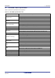
2. List of Abbreviations and Acronyms Abbreviation Full Form Arduino™ UNO Connectors compatible with the Arduino™ UNO R3 board are mounted on the fast prototyping board. BLE Bluetooth Low Energy The Bluetooth® word mark and logos are registered trademarks owned by Bluetooth SIG, Inc. and any use of such marks by Renesas Electronics Corporation is under license.
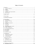
Table of Contents 1. Overview............................................................................................................................ 7 1.1 1.2 1.3 1.4 1.5 1.6 Package Components ................................................................................................................................ 7 Purpose ...................................................................................................................................................... 7 Features ...........
EK-RA4W1 1. Overview 1. Overview 1.1 Package Components Thank you for purchasing the EK-RA4W1 evaluation tool from Renesas (hereinafter referred to as “this product”). This product consists of the EK-RA4W1 (RTK7EKA4W1S00000BJ). 1.2 Purpose This product is an evaluation tool for a Renesas MCU. This user’s manual describes the hardware specifications, the method of setting the switches on the board, and the basic procedures for setting this product up. 1.
EK-RA4W1 1.5 1. Overview EK-RA4W1: Table of Specifications Table 1-1 shows the specifications of this product. Table 1-1 EK-RA4W1 Specification Table Item Specification Part No.: R7FA4W1AD2CNG Evaluation MCU Package: 56-pin QFN On-chip memory: 512-KB ROM, 96-KB RAM, 8-KB data flash memory Size: 54.0 mm x 90.0 mm Board size Thickness: 1.6 mm USB connector: 5-V input Power-supply voltage Power-supply IC: 5-V input, 3.3-V output External power-supply header*1: 3.
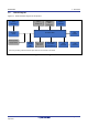
EK-RA4W1 1.6 1. Overview Block Diagram Figure 1-1 shows the block diagram of this product. USB connector MCU header x 2 Emulator circuit External powersupply header Arduino™ UNO connector Pmod™ connector BLE antenna Evaluation MCU Power indicator LED Main clock Sub-clock Reset switch User switch User LED x 2 USB serial port USB connector Note: Gray shading of blocks indicates parts that are not mounted on the board. Figure 1-1 Block Diagram R20UT4683EJ0100 Rev.0.90 Apr.28.
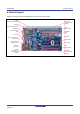
EK-RA4W1 2. Board Layout 2. Board Layout Figure 2-1 shows the external appearance of the top side of this product.
EK-RA4W1 3. Parts Layout 3. Parts Layout Figure 3-1 shows the parts layout of this product. 2.54 mm 54.0 mm 33.02 mm 2.54 mm 90.0 mm Figure 3-1 Parts Layout R20UT4683EJ0100 Rev.0.90 Apr.28.
EK-RA4W1 4. Operating Environment 4. Operating Environment Figure 4-1 shows the operating environment of this product. Install the IDE from the following URL on the host PC. The installer automatically installs all required drivers along with the IDE. https://www.renesas.com/ra/ek-ra4w1 USB cable EK-RA4W1 Host PC Figure 4-1 Operating Environment R20UT4683EJ0100 Rev.0.90 Apr.28.
EK-RA4W1 5. User Circuits 5. User Circuits 5.1 Evaluation MCU The MCU specifications for the power supply, system clock, and reset at the time of shipment are as follows. Power supply: Fixed 3.3 V (including the analog power supply) System clock: Operation with an on-chip oscillator Reset: Directed by the reset switch or IDE 5.2 Bluetooth Low Energy A BLE communications circuit is mounted on this board.
EK-RA4W1 5.3 5. User Circuits Emulator An emulator (J-LINK OB) is mounted on the board. With the settings as shipped, the switches shown in Figure 5-2 are turned off and the emulator is in reset state. To use the emulator, make the corresponding switch setting in Table 5-1. The shape of the emulator connector (ECN1) is USB micro-B for the IDE. Connect the emulator connector to the computer by a USB cable.
EK-RA4W1 5.4 5. User Circuits USB-to-Serial Conversion USB connector CN5 is connected to the USB-to-serial conversion module from FTDI and can be used as a virtual COM port. Table 5-2 shows the connection relationship of USB-to-serial signals.
EK-RA4W1 5.8 5. User Circuits External Power-Supply Header When more current is required than the USB is capable of supplying, use the external power-supply header (J6) to supply power. The usable voltage is 3.3 V. When this header is to be used, remove the pattern for cutting (SS19) on the soldered side, electrically separating the emulator from the target. Figure 5-4 shows the position of the pattern for cutting.
EK-RA4W1 5.9 5. User Circuits Pmod Connector A Pmod connector (CN6) is connectable to the evaluation MCU via a type 2A Pmod interface. Note that the pin assignments of the Pmod connector differ from those of other headers. Figure 5-6 and Table 5-3 show the pin assignments of the Pmod connector and the specifications of signals on the Pmod connector, respectively. The IRQ1 interrupt is multiplexed on the same pin. Figure 5-6 Pin Assignments of the Pmod Connector (Top View) Table 5-3 Pin No.
EK-RA4W1 5.10 5. User Circuits Arduino UNO Headers For the CN1, CN2, CN3, and CN4 headers, through holes are assigned with a pitch of 2.54 mm and these headers are connected to the evaluation MCU according to the Arduino UNO R3 specification. Table 5-4, Table 5-5, Table 5-6, and Table 5-7 show the signal specifications of the Arduino UNO connectors (the actual connector components are not mounted on the board as shipped). Table 5-4 Pin Assignments of CN1 (8-Pin Power Connector) Pin No.
EK-RA4W1 Table 5-6 5. User Circuits Pin Assignments of CN3 (10-Pin Digital Connector) Pin No. Signal Name Specification MCU Signal Name Pin No.
EK-RA4W1 5.11 5. User Circuits Current Measurement Header The current measurement header (J7) is used to measure the current drawn by the evaluation MCU (an actual header component is not mounted on the board as shipped). The current drawn can be measured by connecting an ammeter to the evaluation MCU. When this header is to be used, remove the relevant pattern for cutting (SS20) on the soldered side. Figure 5-7 shows the positions of the header and pattern for cutting.
EK-RA4W1 R20UT4683EJ0100 Rev.0.90 Apr.28.20 5.
EK-RA4W1 6. Configurations 6. Configurations 6.1 Modifying the EK-RA4W1 This section describes how to change the setting of this product by using option-link resistors. An option-link resistor is a 0-Ω surface-mount resistor, which is used to short-circuit or isolate a part of circuits. The subsequent sections contain lists of option-link resistors for individual functions. Fit or remove option-link resistors to switch functions with reference to the list.
EK-RA4W1 6.3 6. Configurations On-Chip Oscillator Table 6-3 and Table 6-4 show the option-link resistors for the operation of the on-chip oscillator. Table 6-3 Option-Link Resistors for the HOCO Setting of the HOCO Mounted Not Mounted Remark Oscillating R5, R9 R6, R8 Halted R6, R8 R5, R9 Mount a crystal oscillator on X1 or X2 and the load capacitance as C8 or C9.
EK-RA4W1 7. Handling Precautions 7. Handling Precautions 7.1 Adding Load When load is added while power is being supplied via the USB, the maximum current is 300 mA during operation at 3.3 V. When load is added while power is being supplied externally, the maximum current is 500 mA regardless of the operating voltage. 7.2 Remodeling the Board Any modification of the board (including removing the patterns for cutting) shall be conducted at the user’s own responsibility. R20UT4683EJ0100 Rev.0.90 Apr.
EK-RA4W1 8. Additional Information 8. Additional Information Technical Support For details on the RA4W1-group microcontrollers, refer to the RA4W1 Group User’s Manual: Hardware. The latest information is available from this Web page: https://www.renesas.com/ra/ek-ra4w1. Technical Contact Details America: techsupport.america@renesas.com Europe: https://www.renesas.com/eu/en/support/contact.html Global & Japan: https://www.renesas.com/support/contact.
EK-RA4W1 9. Certification of Compliance 9. Certification of Compliance The EK-RA4W1 has obtained certificates of compliance with the laws and regulations stated below. Since the use of this product in countries and regions that require compliance with other regulations may lead to the violation of the laws; confirm the regulations of such countries in which the product is to be used. The use of this product in a Faraday-shielded chamber or box may be required. 9.
EK-RA4W1 9. Certification of Compliance FCC Regulatory FCC ID: 2AEMXEKRA4W1Q56 This device complies with part 15 of the FCC Rules. Operation is subject to the following two conditions: (1) This device may not cause harmful interference, and (2) this device must accept any interference received, including interference that may cause undesired operation.
EK-RA4W1 User’s Manual Revision History Rev. Date Description Page 0.90 Apr.28.
EK-RA4W1 User’s Manual Apr.28.20 Publication Date: Rev.0.
RA4W1 Group R20UT4683EJ0100