
User Manual


6
B
C
DD
C
B
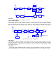
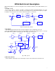
PLL DATA
PLL IC IC1
I/N
5KHz/6.25KHz
PHASE
COMPARATOR
REF OSC
12.8MHz
I/M
5KHz/6.25KHz
CHARGE
LPF
D2.4
Q4
TX VCO
D1.3
Q3
RX VCO
Q6
BUFF AMP
Q5.7
T/R SW
Q2
RF AMP
PUMP
Fig. 4. PLL circuit
2) VCO
The operating frequency is generated by Q4 in transmit mode and Q3 in receive mode. The oscillator
frequency is controlled by applying the VCO control voltage, obtained from the phase comparator, to the
varactor diodes (D2 and D4 in transmit mode and D1 and D3 in receive mode) . The T/R pin is set high in
receive mode causing Q5 and Q7 to turn Q4 off, and turn Q3 on. The T/R pin is set low in transmit mode.
The outputs from Q3 and Q4 are amplified by Q6 and sent to the buffer amplifiers.
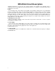
3) UNLOCK DETECTOR
If a pulse signal appears at the LD pin of IC1, an unlock condition occurs, and the DC voltage obtained
from D7, R6, and C1 causes the voltage applied to the UL pin of the microprocessor to go low. When the
microprocessor detects this condition, the transmitter is disabled, ignoring the push-to-talk switch input
signal. (See Fig. 5)
IC1
LD
PLL IC
D7
5C
R6
C1
IC403
UL
MPU
Fig. 5. Unlock detector circuit
4. Transmitter
1) Transmit audio
The modulation signal from the microphone is amplified by IC500 (1/2), passes through a preemphasis
circuit, and amplified by the other IC500 (1/2) to perform IDC operation. The signal then passes through a
low-pass filter (splatter filter) (Q501 and Q502) and cuts 3kHz and higher frequencies.