
User's Manual

RTL8191E-GR
Datasheet
Wireless LAN Network Interface Controller 9 Rev.0.4
5. Pin Descriptions
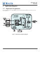
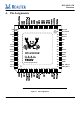
In order to reduce pin count, and therefore size and cost, some pins have multiple functions. In such cases,
the functions are separated with a ‘/’ symbol. Refer to the Pin Assignments diagram on page 10 for a
graphical representation.
The following signal type codes are used in the tables:
I: Input.
O: Output
T/S: Tri-State bi-directional input/output pin.
S/T/S: Sustained Tri-State.
O/D: Open Drain.
P: Power pin.
5.1.
PCIE Transceiver Interface
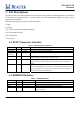
Table 1. PCIE Transceiver Interface
Symbol Type Pin No Description
HSIN/HSIP I 46/47 PCI Express Receive Differential Pair
HSON/HSOP O 42/43 PCI Express Transmit Differential Pair
REFCLK_P/
REFCLK_N
I 44/45 PCI Express Differential Reference Clock Source: 100MHz ± 300ppm
CLKREQn O 34 Reference clock request signal. This signal is used by the RTL8191SE-GR to
request starting of the PCI Express reference clock
WAKEn O/D 33 Power Management Event: Open drain, active low.
Used to reactivate the PCI Express slot’s main power rails and reference
clocks.
PERSTn I 35 PCI Express Reset Signal: Active low.
When the PERSTB is asserted at power-on state, the RTL8191SE-GR returns
to a pre-defined reset state and is ready for initialization and configuration
after the de-assertion of the PERSTB.
5.2.
EEPROM Interface
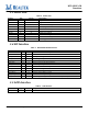
Table 2. EEPROM Interface
Symbol Type Pin No Description
EESK O 62 EESK in 93C46 programming or auto-load mode.
EEDI O 61 EEDI in 93C46 programming or auto-load mode.
EEDO I/O 60 EEDO in 93C46 programming or auto-load mode.
EECS O 63 EEPROM Chip Select.
93C46 chip select.