
User's Manual
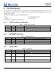
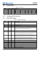
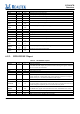
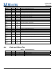
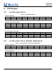
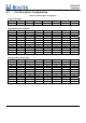
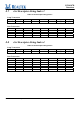
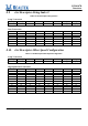
Table Of Contents
- RTL8187B_DataSheet_1.022.pdf
- RTL8187B_DataSheet_1.022.pdf
- RTL8187B_DataSheet_1.022.pdf
- General Description
- Features
- System Applications
- Block Diagram
- Pin Assignments
- Pin Descriptions
- CPU Access to Endpoint Data
- USB Request
- Get Descriptor-Device
- Get Descriptor-Device Qualifier (High Speed)
- Get Descriptor-Configuration
- Get Descriptor-String Index 0
- Get Descriptor-String Index 1
- Get Descriptor-String Index 2
- Get Descriptor-String Index 3
- Get Descriptor-String Index 4
- Get Descriptor-String Index 5
- Get Descriptor-Other Speed Configuration
- Set Address
- Set Interface 0
- Set Feature Device
- Clear Feature Device
- Set Config 0
- Set Config 1
- EEPROM (93C46 or 93C56) Contents
- USB Packet Buffering
- Functional Description
- Application Diagram
- Electrical Characteristics
- Mechanical Dimensions
- Ordering Information
- SGS Test Report
- RTL8187L manual1.pdf
- RTL8187B_DataSheet_1.022.pdf
- RTL8187B_DataSheet_1.022.pdf

RTL8187B
Datasheet
Wireless LAN Network Interface Controller
6
Track ID: JATR-1076-21 Rev. 1.0
6. Pin Descriptions
In order to reduce pin count, and therefore size and cost, some pins have multiple functions. In such cases,
the functions are separated with a ‘/’ symbol. Refer to the Pin Assignments diagram on page 5 for a
graphical representation.
The following signal type codes are used in the tables:
I: Input.
O: Output
T/S: Tri-State bi-directional input/output pin.
S/T/S: Sustained Tri-State.
O/D: Open Drain.
6.1.
USB Transceiver Interface
Table 1. USB Transceiver Interface
Symbol Type Pin No Description
HSDP I/O 26 High speed USB D+ signal
HSDM I/O 24 High speed USB D- signal
RREF N/A 31 External Reference. Requires 1% precision 6.25K resistor to ground
6.2.
EEPROM Interface
Table 2. EEPROM Interface
Symbol Type Pin No Description
EESK O 51 EESK in 93C46 (93C56) programming or auto-load mode.
EEDI O 39 EEDI in 93C46 (93C56) programming or auto-load mode.
EEDO I/O 36 EEDO in 93C46 (93C56) programming or auto-load mode.
EECS O 47 EEPROM Chip Select. 93C46 (93C56) chip select.
6.3.
Power Pins
Table 3. Power Pins
Symbol Type Pin No Description
VCC3 P 40, 59, 78, 93, 111 +3.3V (Digital).
AVDD P 2, 9, 22, 29, 127 +3.3V (Analog).
VCCK P 44, 53, 72, 82, 90, 105,
115
+1.5V.
GNDK P 41, 45, 52, 60, 73, 80,
83, 91, 92, 106, 110,
116
Ground (Digital).
AGND P 3, 10, 21, 23, 30, 123,
126
Ground (Analog).