
Specifications
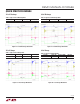
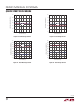
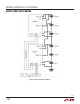
Table Of Contents
6
dc2064af
DEMO MANUAL DC2064A
QUICK START PROCEDURE
Cell Balancer Efficiency Measurements:
Figure 28 shows the proper connections for measuring
the efficiency of a cell balancer. The secondary of the cell
balancer connects to the top of stack. This connection
needs to be to an isolated power source through a current
sensing resistor (0.10Ω). Cells 1 through 6 are connected
to the BOT6_TS turret with its return path the V– turret
while
Cells 7 through 12 are connected to the TOP6_TS
turret with its return path the C6 turret. The primary side
connections of the cell balancers are connected to a string
of batteries that simulate the battery stack. Cell 1 is a 2-wire
connection that connects the positive node, through a
current sensing resistor (0.01Ω), to the C1 turret, and the
negative node to the V– turret. Remote sense connections
for
power sources with remote sensing capabilities should
be connected to the C1 and V– respectively. All other
connections of the simulated string of batteries connect
their positive node, through a current sensing resistor
(0.01Ω), to respective turrets. Cell voltage measurements
should be made across the C(x) and C(x – 1) turrets of
the respective cells. Stack voltage measurements should
be made at the BOT6_TS and TOP6_TS
turrets and their
return path turret.
To calculate cell balancer efficiency use the expressions
below:
Cells 1-6
Charge Mode
Efficiency
1
=
Vm
1
•Vm
2
•10
Vm
3
•Vm
4
•100%
Discharge Mode
Efficiency
1
=
Vm
3
•Vm
4
Vm
1
•Vm
2
•10
•100%
Cells 7-12
Charge Mode
Efficiency
11
=
Vm
5
•Vm
6
•10
Vm
7
•Vm
8
•100%
Discharge Mode
Efficiency
11
=
Vm
7
•Vm
8
Vm
5
•Vm
6
•10
•100%
Cell Balancer Performance Measurements:
Table 2 through Table 5 present the typical operational data
for a 12-cell and 6-cell balancer in both Discharge and
Charge modes. The cell voltages were 3.6V and measure-
ments of Cell Current, Stack Current, Operating Frequency
were taken and transfer Efficiency was calculated from
the data. Figure 12 through Figure 15 are actual in circuit
waveforms taken on Cell 1 and Cell 7 while operating in
both modes.
The waveforms present voltage on the pri-
mary side and secondary side MOSFET’s drain to source
voltage and the primary side and secondary side current
sense inputs to the LTC3300-1.
Figures 16 through 19 are cell and stack currents taken
over a range of cell voltages from 2.6V to 4.0V. The RTONP
and RTONS resistors for these graphs were set for 2.6V
cell voltage operation. All cells were
set to the cell voltage
under test. The slight negative slope in current at higher
voltages is due to the increased operating frequency
and the circuit delays and dead time becoming a higher
percent-age of the operating period.