
Datasheet

06 February 2012 Broadcom Europe Ltd. 406 Science Park Milton Road Cambridge CB4 0WW Page 98
© 2012 Broadcom Corporation. All rights reserved
GPIO Falling Edge Detect Enable Registers (GPRENn)
S
YNOPSIS
The falling edge detect enable registers define the pins for which a falling edge
transition sets a bit in the event detect status registers (GPEDSn). When the relevant
bits are set in both the GPRENn and GPFENn registers, any transition (1 to 0 and 0
to 1) will set a bit in the GPEDSn registers. The GPFENn registers use synchronous
edge detection. This means the input signal is sampled using the system clock and
then it is looking for a “100” pattern on the sampled signal. This has the effect of
suppressing glitches.
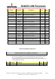
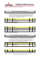
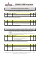
Bit(s) Field Name Description Type Reset
31-0 FENn (n=0..31)
0 =
Falling
edge detect disabled on GPIO pin
n.
1 = Falling edge on GPIO pin n sets corresponding bit in
EDSn.
R/W 0
Table 6-18 – GPIO Falling Edge Detect Status Register 0
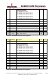
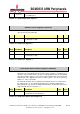
Bit(s) Field Name Description Type Reset
31-22 -
Reserved
R 0
21-0 FENn (n=32..53)
0 =
Falling
edge detect disabled on GPIO pin
n.
1 = Falling edge on GPIO pin n sets corresponding bit in
EDSn.
R/W 0
Table 6-19 – GPIO Falling Edge Detect Status Register 1
GPIO High Detect Enable Registers (GPHENn)
S
YNOPSIS
The high level detect enable registers define the pins for which a high level sets a bit in
the event detect status register (GPEDSn). If the pin is still high when an attempt is
made to clear the status bit in GPEDSn then the status bit will remain set.
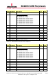
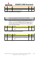
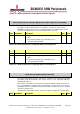
Bit(s) Field Name Description Type Reset
31-0 HENn (n=0..31)
0 = High detect disabled on GPIO pin
n
1 = High on GPIO pin n sets corresponding bit in GPEDS
R/W 0
Table 6-20 – GPIO High Detect Status Register 0
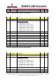
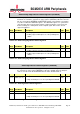
Bit(s) Field Name Description Type Reset
31-22 -
Reserved
R 0
21-0 HENn (n=32..53)
0 = High detect disabled on GPIO pin
n
1 = High on GPIO pin n sets corresponding bit in GPEDS
R/W 0
Table 6-21 – GPIO High Detect Status Register 1