
Datasheet

06 February 2012 Broadcom Europe Ltd. 406 Science Park Milton Road Cambridge CB4 0WW Page 96
© 2012 Broadcom Corporation. All rights reserved
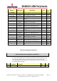
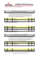
21-0 CLRn
(n=32..53)
0 = No effect
1 = Set GPIO pin n
R/W 0
Table 6-11 – GPIO Output Clear Register 1
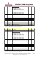
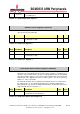
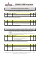
GPIO Pin Level Registers (GPLEVn)
S
YNOPSIS
The pin level registers return the actual value of the pin. The LEV{n} field gives the
value of the respective GPIO pin.
Bit(s) Field Name Description Type Reset
31-0 LEVn (n=0..31)
0 = GPIO pin n is low
0 = GPIO pin n is high
R/W 0
Table 6-12 – GPIO Level Register 0
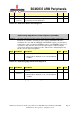
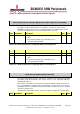
Bit(s) Field Name Description Type Reset
31-22 -
Reserved
R 0
21-0 LEVn (n=32..53)
0 = GPIO pin n is low
0 = GPIO pin n is high
R/W 0
Table 6-13 – GPIO Level Register 1
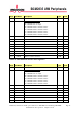
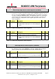
GPIO Event Detect Status Registers (GPEDSn)
S
YNOPSIS
The event detect status registers are used to record level and edge events on the
GPIO pins. The relevant bit in the event detect status registers is set whenever: 1)
an edge is detected that matches the type of edge programmed in the rising/falling
edge detect enable registers, or 2) a level is detected that matches the type of level
programmed in the high/low level detect enable registers. The bit is cleared by
writing a “1” to the relevant bit.
The interrupt controller can be programmed to interrupt the processor when any of
the status bits are set. The GPIO peripheral has three dedicated interrupt lines.
Each GPIO bank can generate an independent interrupt. The third line generates a
single interrupt whenever any bit is set.
Bit(s) Field Name Description Type Reset
31-0 EDSn (n=0..31)
0 = Event not detected on GPIO pin n
1 = Event detected on GPIO pin n
R/W 0
Table 6-14 – GPIO Event Detect Status Register 0