
Datasheet

06 February 2012 Broadcom Europe Ltd. 406 Science Park Milton Road Cambridge CB4 0WW Page 91
© 2012 Broadcom Corporation. All rights reserved
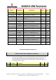
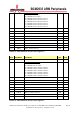
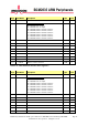
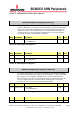
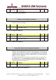
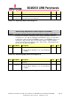
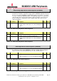
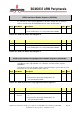
Address Field Name Description Size
Read/
Write
0x 7E20 0060
- Reserved - -
0x 7E20 0064
GPHEN0 GPIO Pin High Detect Enable 0 32 R/W
0x 7E20 0068
GPHEN1 GPIO Pin High Detect Enable 1 32 R/W
0x 7E20 006C
- Reserved - -
0x 7E20 0070
GPLEN0 GPIO Pin Low Detect Enable 0 32 R/W
0x 7E20 0074
GPLEN1 GPIO Pin Low Detect Enable 1 32 R/W
0x 7E20 0078
- Reserved - -
0x 7E20
007C
GPAREN0 GPIO Pin Async. Rising Edge Detect 0 32 R/W
0x 7E20 0080
GPAREN1 GPIO Pin Async. Rising Edge Detect 1 32 R/W
0x 7E20 0084
- Reserved - -
0x 7E20 0088
GPAFEN0 GPIO Pin Async. Falling Edge Detect 0 32 R/W
0x 7E20 008C
GPAFEN1 GPIO Pin Async. Falling Edge Detect 1 32 R/W
0x 7E20 0090
- Reserved - -
0x 7E20 0094
GPPUD GPIO Pin Pull-up/down Enable 32 R/W
0x 7E20 0098
GPPUDCLK0 GPIO Pin Pull-up/down Enable Clock 0 32 R/W
0x 7E20 009C
GPPUDCLK1 GPIO Pin Pull-up/down Enable Clock 1 32 R/W
0x
7E20 00A0
- Reserved - -
0x 7E20 00B0
- Test 4 R/W
Table 6-1 GPIO Register Assignment
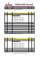
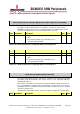
GPIO Function Select Registers (GPFSELn)
S
YNOPSIS
The function select registers are used to define the operation of
the general
-
purpose I/O
pins. Each of the 54 GPIO pins has at least two alternative functions as defined in section
16.2. The FSEL{n} field determines the functionality of the nth GPIO pin. All unused
alternative function lines are tied to ground and will output a “0” if selected. All pins reset
to normal GPIO input operation.
Bit(s) Field Name Description Type Reset
31-30 --- Reserved R 0