
Datasheet

06 February 2012 Broadcom Europe Ltd. 406 Science Park Milton Road Cambridge CB4 0WW Page 85
© 2012 Broadcom Corporation. All rights reserved
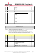
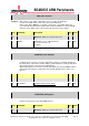
DBG_SEL Register
Synopsis
This register selects which submodules are accessed by the debug bus.
For the exact details please refer to the Arasan documentation
SD3.0_Host_AHB_eMMC4.4_Usersguide_ver5.9_jan11_10.pdf. Bits marked as
reserved in this document but not by the Arasan documentation refer to functionality
which has been disabled due to the changes listed in the previous chapter.
Bit(s)
Field Name
Descri
ption
Type
Reset
31:1
Reserved
-
Write as 0, read as don't care
0 SELECT Submodules accessed by debug bus:
0 = receiver and fifo_ctrl
1 = others
RW 0x0
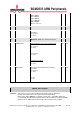
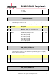
EXRDFIFO_CFG Register
Synopsis
This register allows fine tuning the dma_req generation for paced DMA transfers when
reading from the card. If the extension data FIFO contains less than RD_THRSH 32
bits words dma_req becomes inactive until the card has filled the extension data FIFO
above threshold. This compensates the DMA latency.
When writing data to the card the extension data FIFO feeds into the EMMC module s
FIFO and no fine tuning is required Therefore the RD_THRSH value is in this case
ignored.
Bit(s)
Field Name
Description
Type
Reset
31:3
Reserved
-
Write as 0, read as don't care
2:0 RD_THRSH Read threshold in 32 bits words RW 0x0
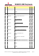
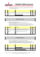
EXRDFIFO_EN Register
Synopsis
This register enables the extension data register. It should be enabled for paced DMA
transfers and be bypassed for burst DMA transfers.
Bit(s)
Field Name
Description
Type
Reset
31:1
Reserved
-
Write as 0, read as don't care