
Datasheet

06 February 2012 Broadcom Europe Ltd. 406 Science Park Milton Road Cambridge CB4 0WW Page 54
© 2012 Broadcom Corporation. All rights reserved
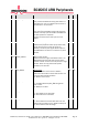
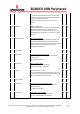
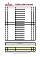
0_STRIDE 1_STRIDE 2_STRIDE 3_STRIDE 4_STRIDE 5_STRIDE 6_STRIDE Register
Synopsis
DMA 2D
Stride
Bit(s)
Field Name
Description
Type
Reset
31:16
D_STRIDE
Destination Stride (2D Mode)
Signed (2 s complement) byte increment to apply to
the destination address at the end of each row in 2D
mode.
RW
0x0
15:0
S_STRIDE
Source Stride (2D Mode)
Signed (2 s complement) byte increment to apply to
the source address at the end of each row in 2D
mode.
RW
0x0
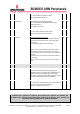
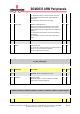
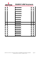
0_NEXTCONBK 1_NEXTCONBK 2_NEXTCONBK 3_NEXTCONBK 4_NEXTCONBK 5_NEXTCONBK
6_NEXTCONBK 7_NEXTCONBK 8_NEXTCONBK 9_NEXTCONBK 10_NEXTCONBK 11_NEXTCONBK
12_NEXTCONBK 13_NEXTCONBK 14_NEXTCONBK Register
Synopsis
DMA Next Control Block Address
The value loaded into this register can be overwritten so that the linked list of Control Block data
structures can be altered. However it is only safe to do this when the DMA is paused. The
address must be 256 bit aligned and so the bottom 5 bits cannot be set and will read back as
zero.
Bit(s)
Field Name
Description
Type
Reset
31:0
ADDR
Address of next CB for chained DMA operations.
RW
0x0
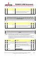
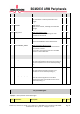
0_DEBUG 1_DEBUG 2_DEBUG 3_DEBUG 4_DEBUG 5_DEBUG 6_DEBUG Register
Synopsis
DMA Debug register.
Bit(s)
Field Name
Description
Type
Reset
31:29
Reserved
-
Write as 0, read as don't care