
Datasheet

06 February 2012 Broadcom Europe Ltd. 406 Science Park Milton Road Cambridge CB4 0WW Page 34
© 2012 Broadcom Corporation. All rights reserved
Synopsis
The clock divider register is used to define the clock speed of the BSC peripheral.
The CDIV field specifies the core clock divider used by the BSC.
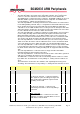
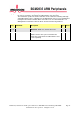
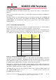
Bit(s)
Field Name
Description
Type
Reset
31:16
Reserved
-
Write as 0, read as don't care
15:0 CDIV Clock Divider
SCL = core clock / CDIV
Where core_clk is nominally 150 MHz. If CDIV is
set to 0, the divisor is 32768. CDIV is always
rounded down to an even number. The default
value should result in a 100 kHz I2C clock
frequency.
RW 0x5dc
DEL Register
Synopsis
The data delay register provides fine control over the sampling/launch point of the
data.
The REDL field specifies the number core clocks to wait after the rising edge before
sampling the incoming data.
The FEDL field specifies the number core clocks to wait after the falling edge before
outputting the next data bit.
Note: Care must be taken in choosing values for FEDL and REDL as it is possible to
cause the BSC master to malfunction by setting values of CDIV/2 or greater. Therefore
the delay values should always be set to less than CDIV/2.
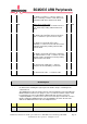
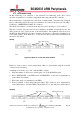
Bit(s)
Field Name
Description
Type
Reset
31:16 FEDL FEDL Falling Edge Delay
Number of core clock cycles to wait after the
falling edge of SCL before outputting next bit of
data.
RW 0x30
15:0 REDL REDL Rising Edge Delay
Number of core clock cycles to wait after the
rising edge of SCL before reading the next bit of
data.
RW 0x30
CLKT Register