
Datasheet


06 February 2012 Broadcom Europe Ltd. 406 Science Park Milton Road Cambridge CB4 0WW Page iii
© 2012 Broadcom Corporation. All rights reserved
8.4.3 DMA 123
8.5 Error Handling. 123
8.6 PDM Input Mode Operation 124
8.7 GRAY Code Input Mode Operation 124
8.8 PCM Register Map 125
9 Pulse Width Modulator 138
9.1 Overview 138
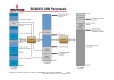
9.2 Block Diagram 138
9.3 PWM Implementation 139
9.4 Modes of Operation 139
9.5 Quick Reference 140
9.6 Control and Status Registers 141
10 SPI 148
10.1 Introduction 148
10.2 SPI Master Mode 148
10.2.1 Standard mode 148
10.2.2 Bidirectional mode 149
10.3 LoSSI mode 150
10.3.1 Command write 150
10.3.2 Parameter write 150
10.3.3 Byte read commands 151
10.3.4 24bit read command 151
10.3.5 32bit read command 151
10.4 Block Diagram 152
10.5 SPI Register Map 152
10.6 Software Operation 158
10.6.1 Polled 158
10.6.2 Interrupt 158
10.6.3 DMA 158
10.6.4 Notes 159
11 SPI/BSC SLAVE 160
11.1 Introduction 160
11.2 Registers 160
12 System Timer 172
12.1 System Timer Registers 172
13 UART 175
13.1 Variations from the 16C650 UART 175
13.2 Primary UART Inputs and Outputs 176
13.3 UART Interrupts 176
13.4 Register View 177
14 Timer (ARM side) 196
14.1 Introduction 196
14.2 Timer Registers: 196
15 USB 200
15.1 Configuration 200
15.2 Extra / Adapted registers. 202