
Datasheet

06 February 2012 Broadcom Europe Ltd. 406 Science Park Milton Road Cambridge CB4 0WW Page 24
© 2012 Broadcom Corporation. All rights reserved
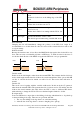
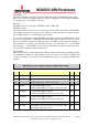
The post-input mode is specifically to deal with this sort of data. If the post-input mode bit is
set, the data arriving at the first falling clock edge is ignored. Then after the last falling clock
edge the CS remain asserted and after a full bit time the last data bit is picked up. The
following figure shows this behaviour:
Clk
Cs_n
Get first bit Get last bit
In this mode the CS will go high 1 full SPI clock cycle after the last clock edge. This
guarantees a full SPI clock cycle time for the data to settle and arrive at the MISO input.
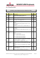
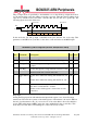
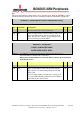
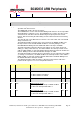
AUXSPI0/1_CNTL1 Register (0x7E21 5084,0x7E21 50C4)
S
YNOPSIS
The
AUXSPIx_CNTL1
registers control more features of the SPI interfaces.
Bit(s)
Field Name Description Type
Reset
31:18
- Reserved, write zero, read as don’t care
10:8
CS high time Additional SPI clock cycles where the CS is high. R/W 0
7
TX empty IRQ
If 1 the interrupt line is high when the transmit FIFO
is empty
R/W 0
6
Done IRQ If 1 the interrupt line is high when the interface is idle
R/W 0
5:2
- Reserved, write zero, read as don’t care
1
Shift in MS bit
first
If 1 the data is shifted in starting with the MS bit. (bit
15)
If 0 the data is shifted in starting with the LS bit. (bit
0)
R/W 0
0 Keep input
If 1 the receiver shift register is NOT cleared. Thus
new data is concatenated to old data.
If 0 the receiver shift register is cleared before each
transaction.
R/W 0
Keep input
Setting the 'Keep input' bit will make that the input shift register is not cleared between
transactions. However the contents of the shift register is still written to the receive FIFO at
the end of each transaction. E.g. if you receive two 8 bit values 0x81 followed by 0x46 the
receive FIFO will contain: 0x0081 in the first entry and 0x8146 in the second entry. This
mode may save CPU time concatenating bits (4 bits followed by 12 bits).