
Datasheet

06 February 2012 Broadcom Europe Ltd. 406 Science Park Milton Road Cambridge CB4 0WW Page 22
© 2012 Broadcom Corporation. All rights reserved
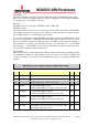
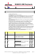
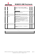
2.3.4 SPI register details.
AUXSPI0/1_CNTL0 Register (0x7E21 5080,0x7E21 50C0)
S
YNOPSIS
The
AUXSPIx_CNTL0
register control many features of the SPI interfaces.
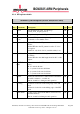
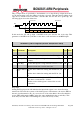
Bit(s)
Field Name Description Type
Reset
31:20
Speed
Sets the SPI clock speed. spi clk freq =
system_clock_freq/2*(speed+1)
R/W 0
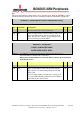
19:17
chip selects The pattern output on the CS pins when active. R/W 111
16
post-input
mode
If set the SPI input works in post input mode.
For details see text further down
R/W 0
15
Variable CS
If 1 the SPI takes the CS pattern and the data from the
TX fifo
If 0 the SPI takes the CS pattern from bits 17-19 of
this register
Set this bit only if also bit 14 (variable width) is set
R/W 0
14
Variable width
If 1 the SPI takes the shift length and the data from
the TX fifo
If 0 the SPI takes the shift length from bits 0-5 of this
register
R/W 0
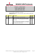
13:12
DOUT Hold
time
Controls the extra DOUT hold time in system clock
cycles.
00 : No extra hold time
01 : 1 system clock extra hold time
10 : 4 system clocks extra hold time
11 : 7 system clocks extra hold time
R/W 0
11
Enable
Enables the SPI interface. Whilst disabled the FIFOs
can still be written to or read from
This bit should be 1 during normal operation.
R/W 0
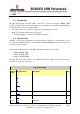
10
In rising
If 1 data is clocked in on the rising edge of the SPI
clock
If 0 data is clocked in on the falling edge of the SPI
clock
R/W 0
9
Clear FIFOs
If 1 the receive and transmit FIFOs are held in reset
(and thus flushed.)
This bit should be 0 during normal operation.
R/W 0