
Datasheet

06 February 2012 Broadcom Europe Ltd. 406 Science Park Milton Road Cambridge CB4 0WW Page 21
© 2012 Broadcom Corporation. All rights reserved
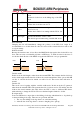
Last there is a guarantee of at least a full bit time where the spi chip select is high. A longer
CS_n high period can be programmed for another 1-7 cycles.
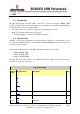
The SPI clock frequency is:
)1_(*2
__
_
+
=
fieldspeed
freqclocksystem
CLKSPIx
If the system clock is 250 MHz and the speed field is zero the SPI clock frequency is 125
MHz. The practical SPI clock will be lower as the I/O pads can not transmit or receive
signals at such high speed. The lowest SPI clock frequency with a 250 MHz system clock is
30.5 KHz.
The hardware has an option to add hold time to the MOSI signal against the SPI clk. This is
again done using the system clock. So a 250 MHz system clock will add hold times in units
of 4 ns. Hold times of 0, 1, 4 and 7 system clock cycles can be used. (So at 250MHz an
additional hold time of 0, 4, 16 and 28 ns can be achieved). The hold time is additional to the
normal output timing as specified in the data sheet.
2.3.2 Interrupts
The SPI block has two interrupts: TX FIFO is empty, SPI is Idle.
TX FIFO is empty:
This interrupt will be asserted as soon as the last entry has been read from the transmit FIFO.
At that time the interface will still be busy shifting out that data. This also implies that the
receive FIFO will not yet contain the last received data. It is possible at that time to fill the
TX FIFO again and read the receive FIFO entries which have been received. Note that there
is no "receive FIFO full" interrupt as the number of entries received is always equal to the
number of entries transmitted.
SPI is IDLE:
This interrupt will be asserted when the transmit FIFO is empty and the SPI block has
finished all actions (including the CS-high time) By this time the receive FIFO will have all
received data as well.
2.3.3 Long bit streams
The SPI module works in bursts of maximum 32 bits. Some SPI devices require data which
is longer the 32 bits. To do this the user must make use of the two different data TX
addresses: Tx data written to one address cause the CS to remain asserted. Tx data written to
the other address cause the CS to be de-asserted at the end of the transmit cycle. So in order
to exchange 96 bits you do the following:
Write the first two data words to one address, then write the third word to the other address.