
Datasheet

06 February 2012 Broadcom Europe Ltd. 406 Science Park Milton Road Cambridge CB4 0WW Page 203
© 2012 Broadcom Corporation. All rights reserved
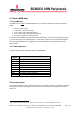
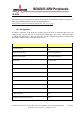
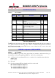
Offset
Address
Description Size
Read/
Write
0x080 USB_MDIO_CNTL
MDIO interface control
R/W
0x084 USB_MDIO_GEN Data for MDIO interface 32 R/W
0x088 USB_VBUS_DRV Vbus and other Miscellaneous controls R/W
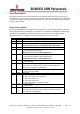
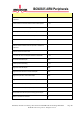
USB MDIO Control (USB_MDIO_CNTL)
Address 0x 7E98 0080
Bit
Number
Field
Name
Description
Read/
Write
Reset
31 mdio_busy 1= MDIO read or write in progress
0= MDIO Idle
R 0
30-24 - Unused - 0
23 bb_mdo Direct write (bitbash) MDO output R/W 0
22 bb_mdc Direct write (bitbash) MDC output R/W 0
21 bb_enbl 1= MDIO bitbash enable
0= MDIO under control of the phy
R/W 0
20 freerun 1= MDC is continous active
0 = MDC only active during data transfer
R/W 0
19:16 mdc_ratio MDC clock freq is sysclk/mdc_ratio R/W 0
15:0 mdi 16-bit read of MDIO input shift register. Updates on
falling edge of MDC
RO 0
Table 15-1 MDIO Control
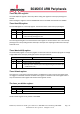
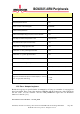
USB MDIO Data (USB_MDIO_DATA)
Address 0x 7E98 0084
Bit
Number
Field
Name
Description
Read/
Write
Reset
31-0 mdio_data 32-bit sequence to send over MDIO bus W 0
31-0 mdio_data 32-bit sequence received from MDIO bus R 0
Table 15-2 USB MDIO data
A Preamble is not auto-generated so any MDIO access must be preceded by a write to this
register of 0xFFFFFFFF. Furthermore, a bug in the USB PHY requires an extra clock edge so
a write of 0x00000000 must follow the actual access.