
Datasheet

06 February 2012 Broadcom Europe Ltd. 406 Science Park Milton Road Cambridge CB4 0WW Page 170
© 2012 Broadcom Corporation. All rights reserved
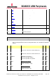
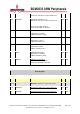
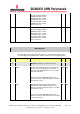
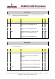
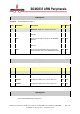
Bit(s)
Field Name
Description
Type
Reset
31:8
Reserved
-
Write as 0, read as don't care
7:0 DATA Test data is written into the receive FIFO and
read out of the transmit FIFO.
RW 0x0
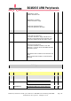
GPUSTAT Register
Synopsis
The GPU SW Status Register to be passed via I2C bus to a Host.
NOTE: GPU SW Status Register is combined with the status bit coming from within
I2C SPI Slave device. Hence, the I2C SPI GPU Host Status Register as it is seen by a
Host is depicted on Table 1 14.
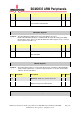
Bit(s)
Field Name
Description
Type
Reset
31:4
Reserved
-
Write as 0, read as don't care
3:0 DATA GPUSTAT GPU to Host Status Register
SW controllable
RW 0x0
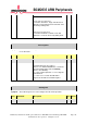
HCTRL Register
Synopsis
The Host Control register is received from the host side via I2C bus. When ENCTRL -
enable control register bit is set, the host control register is received as the first data
character after the I2C address.
Bit(s)
Field Name
Description
Type
Reset
31:8
Reserved
-
Write as 0, read as don't care
7:0 DATA HCTRL Host Control Register
SW processing received via I2C bus
RW 0x0
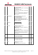
DEBUG1 Register
Synopsis
I2C Debug Register