
Datasheet

06 February 2012 Broadcom Europe Ltd. 406 Science Park Milton Road Cambridge CB4 0WW Page 156
© 2012 Broadcom Corporation. All rights reserved
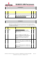
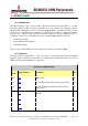
Bit(s)
Field Name
Description
Type
Reset
31:0 DATA DMA Mode (DMAEN set)
If TA is clear, the first 32-bit write to this register
will control SPIDLEN and SPICS. Subsequent
reads and writes will be taken as four-byte data
words to be read/written to the FIFOs
Poll/Interrupt Mode (DMAEN clear, TA set)
Writes to the register write bytes to TX FIFO.
Reads from register read bytes from the RX
FIFO
RW 0x0
CLK Register
Synopsis
This register allows the SPI clock rate to be set.
Bit(s)
Field Name
Description
Type
Reset
31:16
Reserved
-
Write as 0, read as don't care
15:0 CDIV Clock Divider
SCLK = Core Clock / CDIV
If CDIV is set to 0, the divisor is 65536. The
divisor must be a power of 2. Odd numbers
rounded down. The maximum SPI clock rate is
of the APB clock.
RW 0x0
DLEN Register
Synopsis
This register allows the SPI data length rate to be set.
Bit(s)
Field Name
Description
Type
Reset
31:16
Reserved
-
Write as 0, read as don't care
15:0 LEN Data Length
The number of bytes to transfer.
This field is only valid for DMA mode (DMAEN
set) and controls how many bytes to transmit
(and therefore receive).
RW 0x0