
Datasheet

06 February 2012 Broadcom Europe Ltd. 406 Science Park Milton Road Cambridge CB4 0WW Page 155
© 2012 Broadcom Corporation. All rights reserved
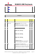
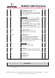
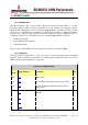
8 DMAEN DMAEN DMA Enable
0 = No DMA requests will be issued.
1 = Enable DMA operation.
Peripheral generates data requests. These will
be taken in four-byte words until the SPIDLEN
has been reached.
RW 0x0
7 TA Transfer Active
0 = Transfer not active./CS lines are all high
(assuming CSPOL = 0). RXR and DONE are 0.
Writes to SPIFIFO write data into bits -0 of
SPICS allowing DMA data blocks to set mode
before sending data.
1 = Transfer active. /CS lines are set according
to CS bits and CSPOL. Writes to SPIFIFO write
data to TX FIFO.TA is cleared by a
dma_frame_end pulse from the DMA controller.
RW 0x0
6 CSPOL Chip Select Polarity
0 = Chip select lines are active low
1 = Chip select lines are active high
RW 0x0
5:4 CLEAR CLEAR FIFO Clear
00 = No action.
x1 = Clear TX FIFO. One shot operation.
1x = Clear RX FIFO. One shot operation.
If CLEAR and TA are both set in the same
operation, the FIFOs are cleared before the new
frame is started. Read back as 0.
RW 0x0
3 CPOL Clock Polarity
0 = Rest state of clock = low.
1 = Rest state of clock = high.
RW 0x0
2 CPHA Clock Phase
0 = First SCLK transition at middle of data bit.
1 = First SCLK transition at beginning of data bit.
RW 0x0
1:0 CS Chip Select
00 = Chip select 0
01 = Chip select 1
10 = Chip select 2
11 = Reserved
RW 0x0
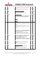
FIFO Register
Synopsis
This register allows TX data to be written to the TX FIFO and RX data to be read from
the RX FIFO.