
Datasheet

06 February 2012 Broadcom Europe Ltd. 406 Science Park Milton Road Cambridge CB4 0WW Page 146
© 2012 Broadcom Corporation. All rights reserved
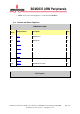
DAT1 Register
Synopsis
This register stores the 32 bit data to be sent by the PWM Controller when USEFi is 0.
In PWM mode data is sent by pulse width modulation: the value of this register defines
the number of pulses which is sent within the period defined by PWM_RNGi. In
serialiser mode data stored in this register is serialised and transmitted.
Note: Channels 3 and 4 are not available in B0 and corresponding Channel Data
Registers are ignored.
Bit(s)
Field Name
Description
Type
Reset
31:0 PWM_DATi Channel i Data RW 0x0
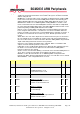
FIF1 Register
Synopsis
This register is the FIFO input for the all channels. Data written to this address is
stored in channel FIFO and if USEFi is enabled for the channel i it is used as data to
be sent. This register is write only, and reading this register will always return bus
default return value, pwm0 .
When more than one channel is enabled for FIFO usage, the data written into the FIFO
is shared between these channels in turn. For example if the word series A B C D E F
G H I .. is written to FIFO and two channels are active and configured to use FIFO then
channel 1 will transmit words A C E G I .. and channel 2 will transmit words B D F H .. .
Note that requesting data from the FIFO is in locked-step manner and therefore
requires tight coupling of state machines of the channels. If any of the channel range
(period) value is different than the others this will cause the channels with small range
values to wait between words hence resulting in gaps between words. To avoid that,
each channel sharing the FIFO should be configured to use the same range value.
Also note that RPTLi are not meaningful when the FIFO is shared between channels
as there is no defined channel to own the last data in the FIFO. Therefore sharing
channels must have their RPTLi set to zero.
If the set of channels to share the FIFO has been modified after a configuration
change, FIFO should be cleared before writing new data.
Bit(s)
Field Name
Description
Type
Reset
31:0 PWM_FIFO Channel FIFO Input RW 0x0
RNG2 Register