
Datasheet

06 February 2012 Broadcom Europe Ltd. 406 Science Park Milton Road Cambridge CB4 0WW Page 126
© 2012 Broadcom Corporation. All rights reserved
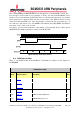
0x18 INTEN_A PCM Interrupt Enables 32
0x1c INTSTC_A PCM Interrupt Status & Clear 32
0x20 GRAY PCM Gray Mode Control 32
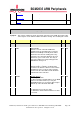
CS_A Register
Synopsis
This register contains the main control and status bits for the PCM. The bottom 3 bits
of this register can be written to whilst the PCM is running. The remaining bits cannot.
Bit(s)
Field Name
Description
Type
Reset
31:26
Reserved
-
Write as 0, read as don't care
25 STBY RAM Standby
This bit is used to control the PCM Rams
standby mode. By default this bit is 0 causing
RAMs to start initially in standby mode. Rams
should be released from standby prior to any
transmit/receive operation. Allow for at least 4
PCM clock cycles to take effect. This may or
may not be implemented, depending upon the
RAM libraries being used.
RW 0x0
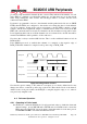
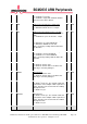
24 SYNC PCM Clock sync helper.
This bit provides a software synchronisation
mechanism to allow the software to detect when
2 PCM clocks have occurred. It takes 2 PCM
clocks before the value written to this bit will be
echoed back in the read value.
RW 0x0
23 RXSEX RX Sign Extend
0 = No sign extension.
1 = Sign extend the RX data. When set, the MSB
of the received data channel (as set by the
CHxWID parameter) is repeated in all the higher
data bits up to the full 32 bit data width.
RW 0x0
22 RXF RX FIFO is Full
0 = RX FIFO can accept more data.
1 = RX FIFO is full and will overflow if more data
is received.
RO 0x0