
Datasheet

06 February 2012 Broadcom Europe Ltd. 406 Science Park Milton Road Cambridge CB4 0WW Page 125
© 2012 Broadcom Corporation. All rights reserved
The normal RXREQ and RXTHR FIFO levels will apply as for normal PCM received data.
If a message is received that is not a multiple of 32 bits, any data in the RX Buffer can be
flushed out by setting the flush bit (FLUSH). Once set, this bit will read back as zero until the
flush operation has completed. This may take several cycles as the APB clock may be many
times faster than the PCM clock. Once the flush has occurred, the bits are packed up to 32
bits with zeros and written out to the RXFIFO. The flushed field (FLUSHED) will indicate
how many of bits of this word are valid.
Note that to get an accurate indication of the number of bits currently in the rx shift register
(RXLEVEL) the APB clock must be at least 2x the PCM_CLK.
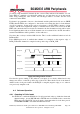
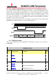
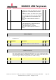
Figure 8-4 Gray mode input format
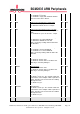
8.8 PCM Register Map
There is only PCM module in the BCM2835. The PCM base address for the registers is
0x7E203000.
PCM Address Map
Address
Offset
Register Name Description Size
0x0 CS_A PCM Control and Status 32
0x4 FIFO_A PCM FIFO Data 32
0x8 MODE_A PCM Mode 32
0xc RXC_A PCM Receive Configuration 32
0x10 TXC_A PCM Transmit Configuration 32
0x14 DREQ_A PCM DMA Request Level 32