
Datasheet

06 February 2012 Broadcom Europe Ltd. 406 Science Park Milton Road Cambridge CB4 0WW Page 120
© 2012 Broadcom Corporation. All rights reserved
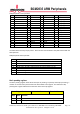
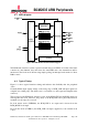
8.1 Block Diagram
Figure 8-2 PCM Audio Interface Block Diagram
The PCM audio interface contains separate transmit and receive FIFOs. Note that if the frame
contains two data channels, they must share the same FIFO and so the channel data will be
interleaved. The block can be driven using simple polling, an interrupt based method or direct
DMA control.
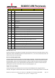
8.2 Typical Timing
Figure 8-1 shows typical interface timing and indicates the flexibility that the peripheral
offers.
Normally PCM output signals change on the rising edge of PCM_CLK and input signals are
sampled on its falling edge. The frame sync is considered as a data signal and sampled in the
same way.
The front end of the PCM audio interface is run off the PCM_CLK and the PCM signals are
timed against this clock. However, the polarity of the PCM_CLK can be physically inverted,
in which case the edges are reversed.
In clock master mode (CLKM=0), the PCM_CLK is an output and is driven from the
PCM_MCLK clock input.
In clock slave mode (CLKM=1), the PCM_CLK is an input, supplied by some external clock
source.