
Datasheet

06 February 2012 Broadcom Europe Ltd. 406 Science Park Milton Road Cambridge CB4 0WW Page 101
© 2012 Broadcom Corporation. All rights reserved
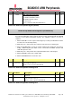
31-2 --- Unused R 0
1-0 PUD PUD - GPIO Pin Pull-up/down
00 = Off – disable pull-up/down
01 = Enable Pull Down control
10 = Enable Pull Up control
11 = Reserved
*Use in conjunction with GPPUDCLK0/1/2
R/W 0
Table 6-28 – GPIO Pull-up/down Register (GPPUD)
GPIO Pull-up/down Clock Registers (GPPUDCLKn)
S
YNOPSIS
The GPIO Pull-up/down Clock Registers control the actuation of internal pull-downs on
the respective GPIO pins. These registers must be used in conjunction with the GPPUD
register to effect GPIO Pull-up/down changes. The following sequence of events is
required:
1. Write to GPPUD to set the required control signal (i.e. Pull-up or Pull-Down or neither
to remove the current Pull-up/down)
2. Wait 150 cycles – this provides the required set-up time for the control signal
3. Write to GPPUDCLK0/1 to clock the control signal into the GPIO pads you wish to
modify – NOTE only the pads which receive a clock will be modified, all others will
retain their previous state.
4. Wait 150 cycles – this provides the required hold time for the control signal
5. Write to GPPUD to remove the control signal
6. Write to GPPUDCLK0/1 to remove the clock
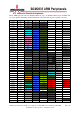
Bit(s) Field Name Description Type Reset
(31-0) PUDCLKn
(n=0..31)
0 = No Effect
1 = Assert Clock on line (n)
*Must be used in conjunction with GPPUD
R/W 0
Table 6-29 – GPIO Pull-up/down Clock Register 0
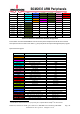
Bit(s) Field Name Description Type Reset
31-22 -
Reserved
R 0
21-0 PUDCLKn (n=32..53) 0 = No Effect
1 = Assert Clock on line (n)
*Must be used in conjunction with GPPUD
R/W 0
Table 6-30 – GPIO Pull-up/down Clock Register 1