BCM2835 ARM Peripherals © 2012 Broadcom Corporation. All rights reserved Broadcom Europe Ltd.
Table of Contents 1 Introduction 1.1 Overview 1.2 Address map 1.2.1 Diagrammatic overview 1.2.2 ARM virtual addresses (standard Linux kernel only) 1.2.3 ARM physical addresses 1.2.4 Bus addresses 1.3 Peripheral access precautions for correct memory ordering 4 4 4 4 6 6 6 7 2 Auxiliaries: UART1 & SPI1, SPI2 2.1 Overview 2.1.1 AUX registers 2.2 Mini UART 2.2.1 Mini UART implementation details. 2.2.2 Mini UART register details. 2.3 Universal SPI Master (2x) 2.3.1 SPI implementation details 2.3.
8.4.3 8.5 8.6 8.7 8.8 DMA Error Handling. PDM Input Mode Operation GRAY Code Input Mode Operation PCM Register Map 123 123 124 124 125 9 Pulse Width Modulator 9.1 Overview 9.2 Block Diagram 9.3 PWM Implementation 9.4 Modes of Operation 9.5 Quick Reference 9.6 Control and Status Registers 138 138 138 139 139 140 141 10 SPI 10.1 10.2 10.2.1 10.2.2 10.3 10.3.1 10.3.2 10.3.3 10.3.4 10.3.5 10.4 10.5 10.6 10.6.1 10.6.2 10.6.3 10.6.
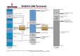
1 Introduction 1.1 Overview BCM2835 contains the following peripherals which may safely be accessed by the ARM: • • • • • • • • • • • Timers Interrupt controller GPIO USB PCM / I2S DMA controller I2C master I2C / SPI slave SPI0, SPI1, SPI2 PWM UART0, UART1 The purpose of this datasheet is to provide documentation for these peripherals in sufficient detail to allow a developer to port an operating system to BCM2835. There are a number of peripherals which are intended to be controlled by the GPU.
06 February 2012 Broadcom Europe Ltd. 406 Science Park Milton Road Cambridge CB4 0WW Page 5 © 2012 Broadcom Corporation.
Addresses in ARM Linux are: • • • • issued as virtual addresses by the ARM core, then mapped into a physical address by the ARM MMU, then mapped into a bus address by the ARM mapping MMU, and finally used to select the appropriate peripheral or location in RAM. 1.2.2 ARM virtual addresses (standard Linux kernel only) As is standard practice, the standard BCM2835 Linux kernel provides a contiguous mapping over the whole of available RAM at the top of memory.
Software accessing RAM directly must use physical addresses (based at 0x00000000). Software accessing RAM using the DMA engines must use bus addresses (based at 0xC0000000). 1.3 Peripheral access precautions for correct memory ordering The BCM2835 system uses an AMBA AXI-compatible interface structure. In order to keep the system complexity low and data throughput high, the BCM2835 AXI system does not always return read data in-order2.
2 Auxiliaries: UART1 & SPI1, SPI2 2.1 Overview The Device has three Auxiliary peripherals: One mini UART and two SPI masters. These three peripheral are grouped together as they share the same area in the peripheral register map and they share a common interrupt. Also all three are controlled by the auxiliary enable register.
0x7E21 50C8 AUX_SPI1_STAT_REG SPI 2 Status 32 0x7E21 50D0 AUX_SPI1_IO_REG SPI 2 Data 32 0x7E21 50D4 AUX_SPI1_PEEK_REG SPI 2 Peek 16 2.1.1 AUX registers There are two Auxiliary registers which control all three devices. One is the interrupt status register, the second is the Auxiliary enable register. The Auxiliary IRQ status register can help to hierarchically determine the source of an interrupt.
If the enable bits are clear you will have no access to a peripheral. You can not even read or write the registers! GPIO pins should be set up first the before enabling the UART. The UART core is build to emulate 16550 behaviour. So when it is enabled any data at the inputs will immediately be received . If the UART1_RX line is low (because the GPIO pins have not been set-up yet) that will be seen as a start bit and the UART will start receiving 0x00-characters.
2.2.1 Mini UART implementation details. The UART1_CTS and UART1_RX inputs are synchronised and will take 2 system clock cycles before they are processed. The module does not check for any framing errors. After receiving a start bit and 8 (or 7) data bits the receiver waits for one half bit time and then starts scanning for the next start bit. The mini UART does not check if the stop bit is high or wait for the stop bit to appear.
AUX_MU_IIR_REG Register (0x7E21 5044) SYNOPSIS Bit(s) The AUX_MU_IER_REG register is primary used to enable interrupts If the DLAB bit in the line control register is set this register gives access to the MS 8 bits of the baud rate. (Note: there is easier access to the baud rate register) Field Name 31:8 7:0 Description Type Reset Reserved, write zero, read as don’t care MS 8 bits Baudrate read/write, DLAB=1 Access to the MS 8 bits of the 16-bit baudrate register.
AUX_MU_IER_REG Register (0x7E21 5048) SYNOPSIS Bit(s) The AUX_MU_IIR_REG register shows the interrupt status. It also has two FIFO enable status bits and (when writing) FIFO clear bits.
AUX_MU_LCR_REG Register (0x7E21 504C) SYNOPSIS Bit(s) The AUX_MU_LCR_REG register controls the line data format and gives access to the baudrate register Field Name Description 31:8 Type Reset Reserved, write zero, read as don’t care 7 DLAB access If set the first to Mini UART register give access the the Baudrate register. During operation this bit must be cleared. R/W 0 6 Break If set high the UART1_TX line is pulled low R/W continuously.
AUX_MU_LSR_REG Register (0x7E21 5054) SYNOPSIS Bit(s) The AUX_MU_LSR_REG register shows the data status. Field Name Description 31:8 Reserved, write zero, read as don’t care 7 Reserved, write zero, read as don’t care This bit has a function in a 16550 compatible UART but is ignored here Type Reset 0 6 Transmitter idle This bit is set if the transmit FIFO is empty and the transmitter is idle. (Finished shifting out the last bit).
AUX_MU_SCRATCH Register (0x7E21 505C) SYNOPSIS Bit(s) The AUX_MU_SCRATCH is a single byte storage. Field Name 31:8 7:0 Description Type Reset Reserved, write zero, read as don’t care One whole byte extra on top of the 134217728 provided by the SDC Scratch R/W 0 AUX_MU_CNTL_REG Register (0x7E21 5060) SYNOPSIS The AUX_MU_CNTL_REG provides access to some extra useful and nice features not found on a normal 16550 UART .
2 Enable receive Auto flowcontrol using RTS If this bit is set the RTS line will de-assert if the receive FIFO reaches it 'auto flow' level. In fact the RTS line will behave as an RTR (Ready To Receive) line. If this bit is clear the RTS line is controlled by the AUX_MU_MCR_REG register bit 1. R/W 0 1 Transmitter enable If this bit is set the mini UART transmitter is enabled.
AUX_MU_STAT_REG Register (0x7E21 5064) SYNOPSIS Bit(s) The AUX_MU_STAT_REG provides a lot of useful information about the internal status of the mini UART not found on a normal 16550 UART.
0 Symbol available If this bit is set the mini UART receive FIFO contains R at least 1 symbol If this bit is clear the mini UART receiver FIFO is empty 0 Receiver is idle This bit is only useful if the receiver is disabled. The normal use is to disable the receiver. Then check (or wait) until the bit is set. Now you can be sure that no new symbols will arrive. (e.g. now you can change the baudrate...) Transmitter is idle This bit tells if the transmitter is idle.
2.3 Universal SPI Master (2x) The two universal SPI masters are secondary low throughput5 SPI interfaces. Like the UART the devices needs to be enabled before they can be used. Each SPI master has the following features: • • • • • • • • • • • Single beat bit length between 1 and 32 bits. Single beat variable bit length between 1 and 24 bits Multi beat infinite bit length. 3 independent chip selects per master. 4 entries 32-bit wide transmit and receive FIFOs. Data out on rising or falling clock edge.
Last there is a guarantee of at least a full bit time where the spi chip select is high. A longer CS_n high period can be programmed for another 1-7 cycles. The SPI clock frequency is: system _ clock _ freq SPIx _ CLK = 2 * ( speed _ field + 1) If the system clock is 250 MHz and the speed field is zero the SPI clock frequency is 125 MHz. The practical SPI clock will be lower as the I/O pads can not transmit or receive signals at such high speed.
2.3.4 SPI register details. AUXSPI0/1_CNTL0 Register (0x7E21 5080,0x7E21 50C0) SYNOPSIS The AUXSPIx_CNTL0 register control many features of the SPI interfaces. Bit(s) Field Name 31:20 Speed Description Type Reset Sets the SPI clock speed. spi clk freq = system_clock_freq/2*(speed+1) R/W 0 19:17 chip selects The pattern output on the CS pins when active. R/W 111 16 post-input mode If set the SPI input works in post input mode.
8 Out rising If 1 data is clocked out on the rising edge of the SPI clock If 0 data is clocked out on the falling edge of the SPI clock R/W 0 7 Invert SPI CLK If 1 the 'idle' clock line state is high. If 0 the 'idle' clock line state is low. R/W 0 6 Shift out MS bit first If 1 the data is shifted out starting with the MS bit. R/W 0 (bit 15 or bit 11) If 0 the data is shifted out starting with the LS bit.
The post-input mode is specifically to deal with this sort of data. If the post-input mode bit is set, the data arriving at the first falling clock edge is ignored. Then after the last falling clock edge the CS remain asserted and after a full bit time the last data bit is picked up. The following figure shows this behaviour: Get first bit Get last bit Clk Cs_n In this mode the CS will go high 1 full SPI clock cycle after the last clock edge.
CS high time The SPI CS will always be high for at least 1 SPI clock cycle. Some SPI devices need more time to process the data. This field will set a longer CS-high time. So the actual CS high time is (CS_high_time + 1) (In SPI clock cycles). Interrupts The SPI block has two interrupts: TX FIFO is empty, SPI is Idle. TX FIFO is empty: This interrupt will be asserted as soon as the last entry has been read from the transmit FIFO. At that time the interface will still be busy shifting out that data.
Busy This status bit indicates if the module is busy. It will be clear when the TX FIFO is empty and the module has finished all activities, including waiting the minimum CS high time. AUXSPI0/1_PEEK Register (0x7E21 508C,0x7E21 50CC) SYNOPSIS The AUXSPIx_PEEK registers show received data of the SPI interfaces. Bit(s) Field Name 31:16 - Description 15:0 Reads from this address will show the top entry from RO the receive FIFO, but the data is not taken from the FIFO.
AUXSPI0/1_TXHOLD Register (0x7E21 50B0-0x7E21 50BC 0x7E21 50F0-0x7E21 50FC) SYNOPSIS The AUXSPIx_TXHOLD registers are the extended CS port of the SPI interfaces These four addresses all write to the same FIFO. Writing to these addresses causes the SPI CS_n pins to remain asserted at the end of the access Bit(s) Field Name Description 31:16 - Reserved, write zero, read as don’t care 15:0 Writes to this address range end up in the transmit R/W 0 FIFO.
3 BSC 3.1 Introduction The Broadcom Serial Controller (BSC) controller is a master, fast-mode (400Kb/s) BSC controller. The Broadcom Serial Control bus is a proprietary bus compliant with the Philips® I2C bus/interface version 2.1 January 2000. • • I2C single master only operation (supports clock stretching wait states) Both 7-bit and 10-bit addressing is supported. • Timing completely software controllable via registers 3.2 Register View The BSC controller has eight memory-mapped registers.
0x1c CLKT Clock Stretch Timeout 32 C Register Synopsis Bit(s) The control register is used to enable interrupts, clear the FIFO, define a read or write operation and start a transfer. The READ field specifies the type of transfer. The CLEAR field is used to clear the FIFO. Writing to this field is a one-shot operation which will always read back as zero. The CLEAR bit can set at the same time as the start transfer bit, and will result in the FIFO being cleared just prior to the start of transfer.
8 INTD INTD Interrupt on DONE 0 = Don t generate interrupts on DONE condition. 1 = Generate interrupt while DONE = 1. RW 0x0 7 ST ST Start Transfer 0 = No action. 1 = Start a new transfer. One shot operation. Read back as 0. RW 0x0 RW 0x0 RW 0x0 Reserved - Write as 0, read as don't care 6 5:4 CLEAR Reserved - Write as 0, read as don't care 3:1 0 CLEAR FIFO Clear 00 = No action. x1 = Clear FIFO. One shot operation. 1x = Clear FIFO. One shot operation.
Synopsis Bit(s) The status register is used to record activity status, errors and interrupt requests. The TA field indicates the activity status of the BSC controller. This read-only field returns a 1 when the controller is in the middle of a transfer and a 0 when idle. The DONE field is set when the transfer completes. The DONE condition can be used with I2CC.INTD to generate an interrupt on transfer completion. The DONE field is reset by writing a 1 , writing a 0 to the field has no effect.
6 TXE TXE - FIFO Empty 0 = FIFO is not empty. 1 = FIFO is empty. If a write is underway, no further serial data can be transmitted until data is written to the FIFO. RO 0x1 5 RXD RXD - FIFO contains Data 0 = FIFO is empty. 1 = FIFO contains at least 1 byte. Cleared by reading sufficient data from FIFO. RO 0x0 4 TXD TXD - FIFO can accept Data 0 = FIFO is full. The FIFO cannot accept more data. 1 = FIFO has space for at least 1 byte.
15:0 DLEN Data Length. Writing to DLEN specifies the number of bytes to be transmitted/received. Reading from DLEN when TA = 1 or DONE = 1, returns the number of bytes still to be transmitted or received. Reading from DLEN when TA = 0 and DONE = 0, returns the last DLEN value written. DLEN can be left over multiple packets. RW 0x0 A Register Synopsis Bit(s) The slave address register specifies the slave address and cycle type.
Synopsis Bit(s) The clock divider register is used to define the clock speed of the BSC peripheral. The CDIV field specifies the core clock divider used by the BSC. Field Name Type Reset RW 0x5dc Reserved - Write as 0, read as don't care 31:16 15:0 Description CDIV Clock Divider SCL = core clock / CDIV Where core_clk is nominally 150 MHz. If CDIV is set to 0, the divisor is 32768. CDIV is always rounded down to an even number. The default value should result in a 100 kHz I2C clock frequency.
Synopsis Bit(s) The clock stretch timeout register provides a timeout on how long the master waits for the slave to stretch the clock before deciding that the slave has hung. The TOUT field specifies the number I2C SCL clocks to wait after releasing SCL high and finding that the SCL is still low before deciding that the slave is not responding and moving the I2C machine forward. When a timeout occurs, the I2CS.CLKT bit is set. Writing 0x0 to TOUT will result in the Clock Stretch Timeout being disabled.
3.3 10 Bit Addressing 10 Bit addressing is an extension to the standard 7-bit addressing mode. This section describes in detail how to read/write using 10-bit addressing with this I2C controller. 10-bit addressing is compatible with, and can be combined with, 7 bit addressing. Using 10 bits for addressing exploits the reserved combination 1111 0xx for the first byte following a START (S) or REPEATED START (Sr) condition.
Figure 3-2 Read from slave with 10 bit address Figure 3-2 shows how a read from a slave with a 10-bit address is performed. Following is the procedure for performing a read using the controller: 1. Write 1 to the I2CDLEN register. 2. Write ‘XXXXXXXX’ to the FIFO where ‘XXXXXXXX’ are the least 8 significant bits of the 10-bit slave address. 3. Write ‘11110XX’ to the Slave Address Register where ‘XX’ are the two most significant bits of the 10-bit address. Set I2CC.READ = 0 and I2CC.
4 DMA Controller 4.1 Overview The majority of hardware pipelines and peripherals within the BCM2835 are bus masters, enabling them to efficiently satisfy their own data requirements. This reduces the requirements of the DMA controller to block-to-block memory transfers and supporting some of the simpler peripherals. In addition, the DMA controller provides a read only prefetch mode to allow data to be brought into the L2 cache in anticipation of its later use.
4.2 DMA Controller Registers The DMA Controller is comprised of several identical DMA Channels depending upon the required configuration. Each individual DMA channel has an identical register map (although LITE channels have less functionality and hence less registers). DMA Channel 0 is located at the address of 0x7E007000, Channel 1 at 0x7E007100, Channel 2 at 0x7E007200 and so on. Thus adjacent DMA Channels are offset by 0x100.
4.2.1 DMA Channel Register Address Map Each DMA channel has an identical register map, only the base address of each channel is different. There is a global enable register at the top of the Address map that can disable each DMA for powersaving. Only three registers in each channels register set are directly writeable (CS, CONBLK_AD and DEBUG). The other registers (TI, SOURCE_AD, DEST_AD, TXFR_LEN, STRIDE & NEXTCONBK), are automatically loaded from a Control Block data structure held in external memory. 4.
Most of the control block registers cannot be written to directly as they loaded automatically from memory. They can be read to provide status information, and to indicate the progress of the current DMA transfer. The value loaded into the NEXTCONBK register can be overwritten so that the linked list of Control Block data structures can be dynamically altered. However it is only safe to do this when the DMA is paused. 4.2.1.
0x118 1_STRIDE DMA Channel 1 CB Word 4 (2D Stride) 32 0x11c 1_NEXTCONBK DMA Channel 1 CB Word 5 (Next CB Address) 32 0x120 1_DEBUG DMA Channel 1 Debug 32 0x200 2_CS DMA Channel 2 Control and Status 32 0x204 2_CONBLK_AD DMA Channel 2 Control Block Address 32 0x208 2_TI DMA Channel 2 CB Word 0 (Transfer Information) 32 0x20c 2_SOURCE_AD DMA Channel 2 CB Word 1 (Source Address) 32 0x210 2_DEST_AD DMA Channel 2 CB Word 2 (Destination Address) 32 0x214 2_TXFR_LEN DMA Channel 2 C
0x400 4_CS DMA Channel 4 Control and Status 32 0x404 4_CONBLK_AD DMA Channel 4 Control Block Address 32 0x408 4_TI DMA Channel 4 CB Word 0 (Transfer Information) 32 0x40c 4_SOURCE_AD DMA Channel 4 CB Word 1 (Source Address) 32 0x410 4_DEST_AD DMA Channel 4 CB Word 2 (Destination Address) 32 0x414 4_TXFR_LEN DMA Channel 4 CB Word 3 (Transfer Length) 32 0x418 4_STRIDE DMA Channel 4 CB Word 4 (2D Stride) 32 0x41c 4_NEXTCONBK DMA Channel 4 CB Word 5 (Next CB Address) 32 0x420 4_
0x60c 6_SOURCE_AD DMA Channel 6 CB Word 1 (Source Address) 32 0x610 6_DEST_AD DMA Channel 6 CB Word 2 (Destination Address) 32 0x614 6_TXFR_LEN DMA Channel 6 CB Word 3 (Transfer Length) 32 0x618 6_STRIDE DMA Channel 6 CB Word 4 (2D Stride) 32 0x61c 6_NEXTCONBK DMA Channel 6 CB Word 5 (Next CB Address) 32 0x620 6_DEBUG DMA Channel 6 Debug 32 0x700 7_CS DMA Channel 7 Control and Status 32 0x704 7_CONBLK_AD DMA Channel 7 Control Block Address 32 0x708 7_TI DMA Channel 7 CB Wor
0x820 8_DEBUG DMA Channel 8 Debug 32 0x900 9_CS DMA Channel 9 Control and Status 32 0x904 9_CONBLK_AD DMA Channel 9 Control Block Address 32 0x908 9_TI DMA Channel 9 CB Word 0 (Transfer Information) 32 0x90c 9_SOURCE_AD DMA Channel 9 CB Word 1 (Source Address) 32 0x910 9_DEST_AD DMA Channel 9 CB Word 2 (Destination Address) 32 0x914 9_TXFR_LEN DMA Channel 9 CB Word 3 (Transfer Length) 32 0x91c 9_NEXTCONBK DMA Channel 9 CB Word 5 (Next CB Address) 32 0x920 9_DEBUG DMA Channe
0xb10 11_DEST_AD DMA Channel 11 CB Word 2 (Destination Address) 32 0xb14 11_TXFR_LEN DMA Channel 11 CB Word 3 (Transfer Length) 32 0xb1c 11_NEXTCONBK DMA Channel 11 CB Word 5 (Next CB Address) 32 0xb20 11_DEBUG DMA Channel 11 Debug 32 0xc00 12_CS DMA Channel 12 Control and Status 32 0xc04 12_CONBLK_AD DMA Channel 12 Control Block Address 32 0xc08 12_TI DMA Channel 12 CB Word 0 (Transfer Information) 32 0xc0c 12_SOURCE_AD DMA Channel 12 CB Word 1 (Source Address) 32 0xc10 12_
0xe04 14_CONBLK_AD DMA Channel 14 Control Block Address 32 0xe08 14_TI DMA Channel 14 CB Word 0 (Transfer Information) 32 0xe0c 14_SOURCE_AD DMA Channel 14 CB Word 1 (Source Address) 32 0xe10 14_DEST_AD DMA Channel 14 CB Word 2 (Destination Address) 32 0xe14 14_TXFR_LEN DMA Channel 14 CB Word 3 (Transfer Length) 32 0xe1c 14_NEXTCONBK DMA Channel 14 CB Word 5 (Next CB Address) 32 0xe20 14_DEBUG DMA Channel 14 Debug 32 0xfe0 INT_STATUS Interrupt status of each DMA channel 32 0x
28 WAIT_FOR_OUTSTANDING_WRITES 27:24 Wait for outstanding writes When set to 1, the DMA will keep a tally of the AXI writes going out and the write responses coming in. At the very end of the current DMA transfer it will wait until the last outstanding write response has been received before indicating the transfer is complete.
6 WAITING_FOR_OUTSTANDING_WRITES DMA is Waiting for the Last Write to be Received Indicates if the DMA is currently waiting for any outstanding writes to be received, and is not transferring data. 1 = DMA channel is waiting. RO 0x0 5 DREQ_STOPS_DMA DMA Paused by DREQ State Indicates if the DMA is currently paused and not transferring data due to the DREQ being inactive.. 1 = DMA channel is paused. 0 = DMA channel is running.
1 END DMA End Flag Set when the transfer described by the current control block is complete. Write 1 to clear. W1C 0x0 0 ACTIVE Activate the DMA This bit enables the DMA. The DMA will start if this bit is set and the CB_ADDR is non zero. The DMA transfer can be paused and resumed by clearing, then setting it again. This bit is automatically cleared at the end of the complete DMA transfer, ie. after a NEXTCONBK = 0x0000_0000 has been loaded.
31:27 Reserved - Write as 0, read as don't care 26 NO_WIDE_BURSTS Don t Do wide writes as a 2 beat burst This prevents the DMA from issuing wide writes as 2 beat AXI bursts. This is an inefficient access mode, so the default is to use the bursts. RW 0x0 25:21 WAITS Add Wait Cycles This slows down the DMA throughput by setting the number of dummy cycles burnt after each DMA read or write operation is completed. A value of 0 means that no wait cycles are to be added.
7 DEST_IGNORE Ignore Writes 1 = Do not perform destination writes. 0 = Write data to destination. RW 0x0 6 DEST_DREQ Control Destination Writes with DREQ 1 = The DREQ selected by PERMAP will gate the destination writes. 0 = DREQ has no effect. RW 0x0 5 DEST_WIDTH Destination Transfer Width 1 = Use 128-bit destination write width. 0 = Use 32-bit destination write width.
Synopsis DMA Source Address Bit(s) Field Name Description Type Reset 31:0 DMA Source Address Source address for the DMA operation. Updated by the DMA engine as the transfer progresses.
0_STRIDE 1_STRIDE 2_STRIDE 3_STRIDE 4_STRIDE 5_STRIDE 6_STRIDE Register Synopsis DMA 2D Stride Bit(s) Field Name Description Type Reset 31:16 D_STRIDE Destination Stride (2D Mode) Signed (2 s complement) byte increment to apply to the destination address at the end of each row in 2D mode. RW 0x0 15:0 S_STRIDE Source Stride (2D Mode) Signed (2 s complement) byte increment to apply to the source address at the end of each row in 2D mode.
28 LITE DMA Lite Set if the DMA is a reduced performance LITE engine. RO 0x0 27:25 VERSION DMA Version DMA version number, indicating control bit filed changes. RO 0x2 24:16 DMA_STATE DMA State Machine State Returns the value of the DMA engines state machine for this channel. RO 0x0 15:8 DMA_ID DMA ID Returns the DMA AXI ID of this DMA channel. RO 0x0 7:4 OUTSTANDING_WRITES DMA Outstanding Writes Counter Returns the number of write responses that have not yet been received.
25:21 WAITS Add Wait Cycles This slows down the DMA throughput by setting the number of dummy cycles burnt after each DMA read or write operation is completed. A value of 0 means that no wait cycles are to be added. RW 0x0 20:16 PERMAP Peripheral Mapping Indicates the peripheral number (1-31) whose ready signal shall be used to control the rate of the transfers, and whose panic signals will be output on the DMA AXI bus. Set to 0 for a continuous un-paced transfer.
4 DEST_INC Destination Address Increment 1 = Destination address increments after each write The address will increment by 4, if DEST_WIDTH=0 else by 32. 0 = Destination address does not change. RW 0x0 3 WAIT_RESP Wait for a Write Response When set this makes the DMA wait until it receives the AXI write response for each write. This ensures that multiple writes cannot get stacked in the AXI bus pipeline. 1= Wait for the write response to be received before proceeding.
31:29 Reserved - Write as 0, read as don't care 28 LITE DMA Lite Set if the DMA is a reduced performance LITE engine. RO 0x1 27:25 VERSION DMA Version DMA version number, indicating control bit filed changes. RO 0x2 24:16 DMA_STATE DMA State Machine State Returns the value of the DMA engines state machine for this channel. RO 0x0 15:8 DMA_ID DMA ID Returns the DMA AXI ID of this DMA channel.
31:16 Reserved - Write as 0, read as don't care 15 INT15 Interrupt status of DMA engine 15 RW 0x0 14 INT14 Interrupt status of DMA engine 14 RW 0x0 13 INT13 Interrupt status of DMA engine 13 RW 0x0 12 INT12 Interrupt status of DMA engine 12 RW 0x0 11 INT11 Interrupt status of DMA engine 11 RW 0x0 10 INT10 Interrupt status of DMA engine 10 RW 0x0 9 INT9 Interrupt status of DMA engine 9 RW 0x0 8 INT8 Interrupt status of DMA engine 8 RW 0x0 7 INT7 Interrupt status of
14 EN14 enable dma engine 14 RW 0x1 13 EN13 enable dma engine 13 RW 0x1 12 EN12 enable dma engine 12 RW 0x1 11 EN11 enable dma engine 11 RW 0x1 10 EN10 enable dma engine 10 RW 0x1 9 EN9 enable dma engine 9 RW 0x1 8 EN8 enable dma engine 8 RW 0x1 7 EN7 enable dma engine 7 RW 0x1 6 EN6 enable dma engine 6 RW 0x1 5 EN5 enable dma engine 5 RW 0x1 4 EN4 enable dma engine 4 RW 0x1 3 EN3 enable dma engine 3 RW 0x1 2 EN2 enable dma engine 2 RW 0x1 1
4.2.1.3 Peripheral DREQ Signals A DREQ (Data Request) mechanism is used to pace the data flow between the DMA and a peripheral. Each peripheral is allocated a permanent DREQ signal. Each DMA channel can select which of the DREQ signals should be used to pace the transfer by controlling the DMA reads, DMA writes or both. Note that DREQ 0 is permanently enabled and can be used if no DREQ is required.
8 BSC/SPI Slave TX 9 BSC/SPI Slave RX 10 unused 11 e.MMC 12 UART TX 13 SD HOST 14 UART RX. 15 DSI 16 SLIMBUS MCTX.
4.3 AXI Bursts The DMA supports bursts under specific conditions. accommodated. Up to 16 beat bursts can be Peripheral (32 bit wide) read bursts are supported. The DMA will generate the burst if there is sufficient room in its read buffer to accommodate all the data from the burst. This limits the burst size to a maximum of 8 beats. Read bursts in destination ignore mode (DEST_IGNORE) are supported as there is no need for the DMA to deal with the data.
1. The internal data structure is 128 bits instead of 256 bits. This means that if you do a 128 bit wide read burst of more than 1 beat, the DMA input register will be full and the read bus will be stalled. The normal DMA engine can accept a read burst of 2 without stalling. If you do a narrow 32 bit read burst from the peripherals then the lite engine can cope with a burst of 4 as opposed to a burst of 8 for the normal engine.
5 External Mass Media Controller o Introduction The External Mass Media Controller (EMMC) is an embedded MultiMedia™ and SD™ card interface provided by Arasan™. It is compliant to the following standards: • SD™ Host Controller Standard Specification Version 3.0 Draft 1.0 • SDIO™ card specification version 3.0 • SD™ Memory Card Specification Draft version 3.0 • SD™ Memory Card Security Specification version 1.01 • MMC™ Specification version 3.31,4.2 and 4.
The software is responsible for checking the status bits of the card’s response in order to verify successful processing by the card. In order to transfer data from/to the card register DATA is accessed after configuring the host and sending the according commands to the card using CMDTM. Because the EMMC module doesn’t interpret the commands sent to the card it is important to configure it identical to the card setup using the CONTROL0 register.
0x18 RESP2 Response bits 95 : 64 32 0x1c RESP3 Response bits 127 : 96 32 0x20 DATA Data 32 0x24 STATUS Status 32 0x28 CONTROL0 Host Configuration bits 32 0x2c CONTROL1 Host Configuration bits 32 0x30 INTERRUPT Interrupt Flags 32 0x34 IRPT_MASK Interrupt Flag Enable 32 0x38 IRPT_EN Interrupt Generation Enable 32 0x3c CONTROL2 Host Configuration bits 32 0x50 FORCE_IRPT Force Interrupt Event 32 0x70 BOOT_TIMEOUT Timeout in boot mode 32 0x74 DBG_SEL Debug Bus Co
Synopsis This register contains the argument for the SD card specific command ACMD23 (SET_WR_BLK_ERASE_COUNT). ARG2 must be set before the ACMD23 command is issued using the CMDTM register. Bit(s) Field Name Description Type Reset 31:0 ARGUMENT Argument to be issued with ACMD23 RW 0x0 BLKSIZECNT Register Synopsis This register must not be accessed or modified while any data transfer between card and host is ongoing. It contains the number and size in bytes for data blocks to be transferred.
CMDTM Register Synopsis Bit(s) This register is used to issue commands to the card. Besides the command it also contains flags informing the EMMC module what card response and type of data transfer to expect. Incorrect flags will result in strange behaviour. For data transfers two modes are supported: either transferring a single block of data or several blocks of the same size.
Reserved - Write as 0, read as don't care 15:6 5 TM_MULTI_BLOCK Type of data transfer 0 = single block 1 = multiple block RW 0x0 4 TM_DAT_DIR Direction of data transfer: 0 = from host to card 1 = from card to host RW 0x0 3:2 TM_AUTO_CMD_EN Select the command to be send after completion of a data transfer: 00 = no command 01 = command CMD12 10 = command CMD23 11 = reserved RW 0x0 1 TM_BLKCNT_EN Enable the block counter for multiple block transfers: 0 = disabled 1 = enabled RW 0x0 Reserve
Bit(s) Field Name Description Type Reset 31:0 RESPONSE Bits 63:32 of the card s response RW 0x0 RESP2 Register Synopsis In case of commands CMD2 and CMD10 this register contains CID[95:64] and in case of command CMD9 it contains CSD[95:64]. Note: this register is only valid once the last command has completed and no new command was issued.
STATUS Register Synopsis Bit(s) This register contains information intended for debugging. Its values change automatically according to the hardware. As it involves resynchronisation between different clock domains it changes only after some latency and it is easy sample the values too early. Therefore it is not recommended to use this register for polling. Instead use the INTERRUPT register which implements a handshake mechanism which makes it impossible to miss a change when polling.
CONTROL0 Register Synopsis Bit(s) This register is used to configure the EMMC module. For the exact details please refer to the Arasan documentation SD3.0_Host_AHB_eMMC4.4_Usersguide_ver5.9_jan11_10.pdf. Bits marked as reserved in this document but not by the Arasan documentation refer to functionality which has been disabled due to the changes listed in the previous chapter.
Reserved - Write as 0, read as don't care 4:3 2 HCTL_HS_EN Select high speed mode (i.e. DAT and CMD lines change on the rising CLK edge): 0 = disabled 1 = enabled RW 0x0 1 HCTL_DWIDTH Use 4 data lines: 0 = disabled 1 = enabled RW 0x0 Reserved - Write as 0, read as don't care 0 CONTROL1 Register Synopsis Bit(s) This register is used to configure the EMMC module. For the exact details please refer to the Arasan documentation SD3.0_Host_AHB_eMMC4.4_Usersguide_ver5.9_jan11_10.pdf.
7:6 CLK_FREQ_MS2 SD clock base divider MSBs RW 0x0 5 CLK_GENSEL Mode of clock generation: 0 = divided 1 = programmable RW 0x0 Reserved - Write as 0, read as don't care 4:3 2 CLK_EN SD clock enable: 0 = disabled 1 = enabled RW 0x0 1 CLK_STABLE SD clock stable: 0 = no 1 = yes RO 0x0 0 CLK_INTLEN Clock enable for internal EMMC clocks for power saving: 0 = disabled 1 = enabled RW 0x0 INTERRUPT Register Synopsis Bit(s) This register holds the interrupt flags.
21 DCRC_ERR Data CRC error: 0 = no error 1 = error RW 0x0 20 DTO_ERR Timeout on data line: 0 = no error 1 = error RW 0x0 19 CBAD_ERR Incorrect command index in response: 0 = no error 1 = error RW 0x0 18 CEND_ERR End bit on command line not 1: 0 = no error 1 = error RW 0x0 17 CCRC_ERR Command CRC error: 0 = no error 1 = error RW 0x0 16 CTO_ERR Timeout on command line: 0 = no error 1 = error RW 0x0 15 ERR An error has occured: 0 = no error 1 = error RO 0x0 14 ENDBOOT Boot
5 READ_RDY DATA register contains data to be read: 0 = no 1 = yes RW 0x0 4 WRITE_RDY Data can be written to DATA register: 0 = no 1 = yes RW 0x0 Reserved - Write as 0, read as don't care 3 2 BLOCK_GAP Data transfer has stopped at block gap: 0 = no 1 = yes RW 0x0 1 DATA_DONE Data transfer has finished: 0 = no 1 = yes RW 0x0 0 CMD_DONE Command has finished: 0 = no 1 = yes RW 0x0 IRPT_MASK Register Synopsis Bit(s) This register is used to mask the interrupt flags in the INTERRUPT re
21 DCRC_ERR Set flag if data CRC error: 0 = no 1 = yes RW 0x0 20 DTO_ERR Set flag if timeout on data line: 0 = no 1 = yes RW 0x0 19 CBAD_ERR Set flag if incorrect command index in response: 0 = no 1 = yes RW 0x0 18 CEND_ERR Set flag if end bit on command line not 1: 0 = no 1 = yes RW 0x0 17 CCRC_ERR Set flag if command CRC error: 0 = no 1 = yes RW 0x0 16 CTO_ERR Set flag if timeout on command line: 0 = no 1 = yes RW 0x0 Reserved - Write as 0, read as don't care 15 14 ENDBOOT
4 WRITE_RDY Set flag if data can be written to DATA register: 0 = no 1 = yes RW 0x0 Reserved - Write as 0, read as don't care 3 2 BLOCK_GAP Set flag if data transfer has stopped at block gap: 0 = no 1 = yes RW 0x0 1 DATA_DONE Set flag if data transfer has finished: 0 = no 1 = yes RW 0x0 0 CMD_DONE Set flag if command has finished: 0 = no 1 = yes RW 0x0 IRPT_EN Register Synopsis Bit(s) This register is used to enable the different interrupts in the INTERRUPT register to generate an int
20 DTO_ERR Create interrupt if timeout on data line: 0 = no 1 = yes RW 0x0 19 CBAD_ERR Create interrupt if incorrect command index in response: 0 = no 1 = yes RW 0x0 18 CEND_ERR Create interrupt if end bit on command line not 1: 0 = no 1 = yes RW 0x0 17 CCRC_ERR Create interrupt if command CRC error: 0 = no 1 = yes RW 0x0 16 CTO_ERR Create interrupt if timeout on command line: 0 = no 1 = yes RW 0x0 Reserved - Write as 0, read as don't care 15 14 ENDBOOT Create interrupt if boot o
4 WRITE_RDY Create interrupt if data can be written to DATA register: 0 = no 1 = yes RW 0x0 Reserved - Write as 0, read as don't care 3 2 BLOCK_GAP Create interrupt if data transfer has stopped at block gap: 0 = no 1 = yes RW 0x0 1 DATA_DONE Create interrupt if data transfer has finished: 0 = no 1 = yes RW 0x0 0 CMD_DONE Create interrupt if command has finished: 0 = no 1 = yes RW 0x0 CONTROL2 Register Synopsis Bit(s) This register is used to enable the different interrupts in the INTE
18:16 UHSMODE RW 0x0 RO 0x0 Reserved - Write as 0, read as don't care 15:8 7 Select the speed mode of the SD card: 000 = SDR12 001 = SDR25 010 = SDR50 011 = SDR104 100 = DDR50 other = reserved NOTC12_ERR Error occurred during auto command CMD12 execution: 0 = no error 1 = error Reserved - Write as 0, read as don't care 6:5 4 ACBAD_ERR Command index error occurred during auto command execution: 0 = no error 1 = error RO 0x0 3 ACEND_ERR End bit is not 1 during auto command execution: 0 = no
Bit(s) Field Name Type Reset RW 0x0 Reserved - Write as 0, read as don't care 31:25 24 Description ACMD_ERR Create auto command error: 0 = no 1 = yes Reserved - Write as 0, read as don't care 23 22 DEND_ERR Create end bit on data line not 1: 0 = no 1 = yes RW 0x0 21 DCRC_ERR Create data CRC error: 0 = no 1 = yes RW 0x0 20 DTO_ERR Create timeout on data line: 0 = no 1 = yes RW 0x0 19 CBAD_ERR Create incorrect command index in response: 0 = no 1 = yes RW 0x0 18 CEND_ERR Create
12 RETUNE RW 0x0 RW 0x0 Reserved - Write as 0, read as don't care 11:9 8 Create clock retune request was made: 0 = no 1 = yes CARD Create card made interrupt request: 0 = no 1 = yes Reserved - Write as 0, read as don't care 7:6 5 READ_RDY Create DATA register contains data to be read: 0 = no 1 = yes RW 0x0 4 WRITE_RDY Create data can be written to DATA register: 0 = no 1 = yes RW 0x0 Reserved - Write as 0, read as don't care 3 2 BLOCK_GAP Create interrupt if data transfer has stopped
DBG_SEL Register Synopsis Bit(s) This register selects which submodules are accessed by the debug bus. For the exact details please refer to the Arasan documentation SD3.0_Host_AHB_eMMC4.4_Usersguide_ver5.9_jan11_10.pdf. Bits marked as reserved in this document but not by the Arasan documentation refer to functionality which has been disabled due to the changes listed in the previous chapter.
0 ENABLE Enable the extension FIFO: 0 = bypass 1 = enabled RW 0x0 TUNE_STEP Register Synopsis Bit(s) This register is used to delay the card clock when sampling the returning data and command response from the card. DELAY determines by how much the sampling clock is delayed per step.
Synopsis Bit(s) This register is used to delay the card clock when sampling the returning data and command response from the card. It determines by how many steps the sampling clock is delayed in DDR mode. Field Name Type Reset RW 0x0 Reserved - Write as 0, read as don't care 31:6 5:0 Description STEPS Number of steps (0 to 40) SPI_INT_SPT Register Synopsis Bit(s) This register controls whether assertion of interrupts in SPI mode is possible independent of the card select line.
Reserved - Write as 0, read as don't care 15:8 7:0 SLOT_STATUS Logical OR of interrupt and wakeup signal for each slot RW 06 February 2012 Broadcom Europe Ltd. 406 Science Park Milton Road Cambridge CB4 0WW © 2012 Broadcom Corporation.
6 General Purpose I/O (GPIO) There are 54 general-purpose I/O (GPIO) lines split into two banks. All GPIO pins have at least two alternative functions within BCM. The alternate functions are usually peripheral IO and a single peripheral may appear in each bank to allow flexibility on the choice of IO voltage. Details of alternative functions are given in section 6.2. Alternative Function Assignments.
The GPIO peripheral has three dedicated interrupt lines. These lines are triggered by the setting of bits in the event detect status register. Each bank has its’ own interrupt line with the third line shared between all bits. The Alternate function table also has the pull state (pull-up/pull-down) which is applied after a power down. 6.1 Register View The GPIO has 41 registers. All accesses are assumed to be 32-bit.
Size Read/ Write - - GPIO Pin High Detect Enable 0 32 R/W GPIO Pin High Detect Enable 1 32 R/W - - GPIO Pin Low Detect Enable 0 32 R/W GPIO Pin Low Detect Enable 1 32 R/W - - GPIO Pin Async. Rising Edge Detect 0 32 R/W GPIO Pin Async. Rising Edge Detect 1 32 R/W - - GPIO Pin Async. Falling Edge Detect 0 32 R/W GPIO Pin Async.
29-27 FSEL9 FSEL9 - Function Select 9 000 = GPIO Pin 9 is an input 001 = GPIO Pin 9 is an output 100 = GPIO Pin 9 takes alternate function 0 101 = GPIO Pin 9 takes alternate function 1 110 = GPIO Pin 9 takes alternate function 2 111 = GPIO Pin 9 takes alternate function 3 011 = GPIO Pin 9 takes alternate function 4 010 = GPIO Pin 9 takes alternate function 5 R/W 0 26-24 FSEL8 FSEL8 - Function Select 8 R/W 0 23-21 FSEL7 FSEL7 - Function Select 7 R/W 0 20-18 FSEL6 FSEL6 - Function Select 6 R
Bit(s) Field Name 31-30 --- 29-27 FSEL29 26-24 Description Reserved Type Reset R 0 FSEL29 - Function Select 29 000 = GPIO Pin 29 is an input 001 = GPIO Pin 29 is an output 100 = GPIO Pin 29 takes alternate function 0 101 = GPIO Pin 29 takes alternate function 1 110 = GPIO Pin 29 takes alternate function 2 111 = GPIO Pin 29 takes alternate function 3 011 = GPIO Pin 29 takes alternate function 4 010 = GPIO Pin 29 takes alternate function 5 R/W 0 FSEL28 FSEL28 - Function Select 28 R/W 0 23-21
5-3 FSEL31 FSEL31 - Function Select 31 R/W 0 2-0 FSEL30 FSEL30 - Function Select 30 R/W 0 Table 6-5 – GPIO Alternate function select register 3 Bit(s) Field Name 31-30 --- 29-27 FSEL49 26-24 Description Reserved Type Reset R 0 FSEL49 - Function Select 49 000 = GPIO Pin 49 is an input 001 = GPIO Pin 49 is an output 100 = GPIO Pin 49 takes alternate function 0 101 = GPIO Pin 49 takes alternate function 1 110 = GPIO Pin 49 takes alternate function 2 111 = GPIO Pin 49 takes alternate functi
Table 6-7 – GPIO Alternate function select register 5 GPIO Pin Output Set Registers (GPSETn) SYNOPSIS The output set registers are used to set a GPIO pin. The SET{n} field defines the respective GPIO pin to set, writing a “0” to the field has no effect. If the GPIO pin is being used as in input (by default) then the value in the SET{n} field is ignored. However, if the pin is subsequently defined as an output then the bit will be set according to the last set/clear operation.
21-0 CLRn (n=32..53) 0 = No effect 1 = Set GPIO pin n R/W 0 Table 6-11 – GPIO Output Clear Register 1 GPIO Pin Level Registers (GPLEVn) SYNOPSIS The pin level registers return the actual value of the pin. The LEV{n} field gives the value of the respective GPIO pin. Bit(s) Field Name 31-0 LEVn (n=0..31) Description 0 = GPIO pin n is low 0 = GPIO pin n is high Type R/W Reset 0 Table 6-12 – GPIO Level Register 0 Bit(s) Field Name 31-22 21-0 - Description Reserved LEVn (n=32..
Bit(s) Field Name 31-22 - 21-0 EDSn (n=32..53) Description Type Reserved 0 = Event not detected on GPIO pin n 1 = Event detected on GPIO pin n Reset R 0 R/W 0 Table 6-15 – GPIO Event Detect Status Register 1 GPIO Rising Edge Detect Enable Registers (GPRENn) SYNOPSIS The rising edge detect enable registers define the pins for which a rising edge transition sets a bit in the event detect status registers (GPEDSn).
GPIO Falling Edge Detect Enable Registers (GPRENn) SYNOPSIS The falling edge detect enable registers define the pins for which a falling edge transition sets a bit in the event detect status registers (GPEDSn). When the relevant bits are set in both the GPRENn and GPFENn registers, any transition (1 to 0 and 0 to 1) will set a bit in the GPEDSn registers. The GPFENn registers use synchronous edge detection.
GPIO Low Detect Enable Registers (GPLENn) SYNOPSIS The low level detect enable registers define the pins for which a low level sets a bit in the event detect status register (GPEDSn). If the pin is still low when an attempt is made to clear the status bit in GPEDSn then the status bit will remain set. Bit(s) Field Name 31-0 LENn (n=0..
Table 6-25 – GPIO Asynchronous rising Edge Detect Status Register 1 GPIO Asynchronous Falling Edge Detect Enable Registers (GPAFENn) SYNOPSIS The asynchronous falling edge detect enable registers define the pins for which a asynchronous falling edge transition sets a bit in the event detect status registers (GPEDSn). Asynchronous means the incoming signal is not sampled by the system clock. As such falling edges of very short duration can be detected. Bit(s) Field Name 31-0 AFENn (n=0..
31-2 --- Unused 1-0 PUD PUD - GPIO Pin Pull-up/down 00 = Off – disable pull-up/down 01 = Enable Pull Down control 10 = Enable Pull Up control 11 = Reserved *Use in conjunction with GPPUDCLK0/1/2 R 0 R/W 0 Table 6-28 – GPIO Pull-up/down Register (GPPUD) GPIO Pull-up/down Clock Registers (GPPUDCLKn) SYNOPSIS The GPIO Pull-up/down Clock Registers control the actuation of internal pull-downs on the respective GPIO pins.
6.2 Alternative Function Assignments Every GPIO pin can carry an alternate function. Up to 6 alternate function are available but not every pin has that many alternate functions. The table below gives a quick over view.
GPIO41 Low PWM1 SD5 SPI2_MOSI RXD1 GPIO42 Low GPCLK1 SD6 SPI2_SCLK RTS1 GPIO43 Low GPCLK2 SD7 SPI2_CE0_N CTS1 GPIO44 - GPCLK1 SDA0 SDA1 SPI2_CE1_N GPIO45 - PWM1 SCL0 SCL1 SPI2_CE2_N GPIO46 High GPIO47 High GPIO48 High GPIO49 High GPIO50 High GPIO51 High GPIO52 High GPIO53 High
Name SPI1_CEx_N SPI1_MISO SPI1_MOSI SPI1_SCLK TXD0 RXD0 CTS0 RTS0 SPI2_CEx_N SPI2_MISO SPI2_MOSI SPI2_SCLK ARM_TRST ARM_RTCK ARM_TDO ARM_TCK ARM_TDI ARM_TMS Function SPI1 Chip select 0-2 SPI1 MISO SPI1 MOSI SPI1 Serial clock UART 1 Transmit Data UART 1 Receive Data UART 1 Clear To Send UART 1 Request To Send SPI2 Chip select 0-2 SPI2 MISO SPI2 MOSI SPI2 Serial clock ARM JTAG reset ARM JTAG return clock ARM JTAG Data out ARM JTAG Clock ARM JTAG Data in ARM JTAG Mode select See section Auxiliary I/O Auxilia
6.3 General Purpose GPIO Clocks The General Purpose clocks can be output to GPIO pins. They run from the peripherals clock sources and use clock generators with noise-shaping MASH dividers. These allow the GPIO clocks to be used to drive audio devices.
Operating Frequency The maximum operating frequency of the General Purpose clocks is ~125MHz at 1.2V but this will be reduced if the GPIO pins are heavily loaded or have a capacitive load. 06 February 2012 Broadcom Europe Ltd. 406 Science Park Milton Road Cambridge CB4 0WW © 2012 Broadcom Corporation.
Register Definitions Clock Manager General Purpose Clocks Control (CM_GP0CTL, GP1CTL & GP2CTL) Address 0x 7e10 1070 CM_GP0CTL 0x 7e10 1078 CM_GP1CTL 0x 7e10 1080 CM_GP2CTL Bit Number Field Name 31-24 23-11 PASSWD - 10-9 MASH Description Clock Manager password “5a” Unused MASH control Read/ Reset Write W R 0 0 R/W 0 R/W 0 R 0 Unused Kill the clock generator R R/W 0 0 0 = no action 1 = stop and reset the clock generator This is intended for test/debug only.
Table 6-34 General Purpose Clocks Control Clock Manager General Purpose Clock Divisors (CM_GP0DIV, CM_GP1DIV & CM_GP2DIV) Address 0x 7e10 1074 CM_GP0DIV 0x 7e10 107c CM_GP1DIV 0x 7e10 1084 CM_GP2DIV Bit Number Field Name 31-24 23-12 PASSWD DIVI 11-0 DIVF Description Read/ Reset Write Clock Manager password “5a” Integer part of divisor W R/W 0 0 This value has a minimum limit determined by the MASH setting. See text for details.
7 Interrupts 7.1 Introduction The ARM has two types of interrupt sources: 1. Interrupts coming from the GPU peripherals. 2. Interrupts coming from local ARM control peripherals. The ARM processor gets three types of interrupts: 1. Interrupts from ARM specific peripherals. 2. Interrupts from GPU peripherals. 3. Special events interrupts. The ARM specific interrupts are: • One timer. • One Mailbox. • Two Doorbells. • Two GPU halted interrupts.
7.2 Interrupt pending. An interrupt vector module has NOT been implemented. To still have adequate interrupt processing the interrupt pending bits are organized as follows: GPU IRQs 32-63 GPU pend. 1 See text VC IRQs 0-31 GPU pend. 0 A few selected GPU IRQs Basic pend. ARM IRQs There are three interrupt pending registers. One basic pending register and two GPU pending registers. Basic pending register. The basic pending register has interrupt pending bits for the ARM specific interrupts .
registers. It is up to the ARM software to device a strategy. e.g. First start looking for specific pending bits or process them all shifting one bit at a time. As interrupt may arrive whilst this process is ongoing the usual care for any 'race-condition critical' code must be taken. The following ARM assembly code has been proven to work: .macro get_irqnr_preamble, base, tmp ldr \base, =IO_ADDRESS(ARMCTRL_IC_BASE) .endm .macro get_irqnr_and_base, irqnr, irqstat, base, tmp ldr \irqstat, [\base, #(ARM_IR
.endm 7.5 Registers The base address for the ARM interrupt register is 0x7E00B000. Registers overview: Address Name Notes offset7 0x200 IRQ basic pending 0x204 IRQ pending 1 0x208 IRQ pending 2 0x20C FIQ control 0x210 Enable IRQs 1 0x214 Enable IRQs 2 0x218 Enable Basic IRQs 0x21C Disable IRQs 1 0x220 Disable IRQs 2 0x224 Disable Basic IRQs The following is a table which lists all interrupts which can come from the peripherals which can be handled by the ARM.
ARM peripherals interrupts table. # 0 1 2 3 4 5 6 7 8 9 10 11 12 13 14 15 IRQ 0-15 # 16 17 18 19 20 21 22 23 24 25 26 27 28 29 30 31 IRQ 16-31 Aux int # 32 33 34 35 36 37 38 39 40 41 42 43 44 45 46 47 IRQ 32-47 i2c_spi_slv_int pwa0 pwa1 # 48 49 50 51 52 53 54 55 56 57 58 59 60 61 62 63 IRQ 48-63 smi gpio_int[0] gpio_int[1] gpio_int[2] gpio_int[3] i2c_int spi_int pcm_int uart_int The table above has many empty entries. These should not be enabled as they will interfere with the GPU operation.
Name: IRQ pend base Address: 0x200 Reset: 0x000 19 R GPU IRQ 57 18 R GPU IRQ 56 17 R GPU IRQ 55 16 R GPU IRQ 54 15 R GPU IRQ 53 14 R GPU IRQ 19 13 R GPU IRQ 18 12 R GPU IRQ 10 11 R GPU IRQ 9 10 R GPU IRQ 7 9 R One or more bits set in pending register 2 8 R One or more bits set in pending register 1 7 R Illegal access type 0 IRQ pending 6 R Illegal access type 1 IRQ pending 5 R GPU1 halted IRQ pending 4 R GPU0 halted IRQ pending (Or GPU1 halted if bit 10 of c
seen on the ARM Peripheral bus. The status of that signal can be read from Error/HALT status register bit 2. Illegal access type-1 IRQ (6) This bit indicates that an address/access error is seen in the ARM control has generated an interrupt. That can either be an address bit 29..26 was high or when a burst access was seen on the GPU Peripheral bus. The status of that signal can be read from Error/HALT status register bits 0 and 1.
Name: FIQ Address: 0x20C Reset: 0x000 Bit(s) R/W Function 31:8 R 7 R FIQ enable. Set this bit to 1 to enable FIQ generation. If set to 0 bits 6:0 are don't care. 6:0 R/W Select FIQ Source FIQ Source. The FIQ source values 0-63 correspond to the GPU interrupt table.
Interrupt enable register 2. Name: IRQ enable 2 Bit(s) 31:0 Address: 0x214 R/W Reset: 0x000 Function R/Wbs Set to enable IRQ source 63:32 (See IRQ table above) Writing a 1 to a bit will set the corresponding IRQ enable bit. All other IRQ enable bits are unaffected. Only bits which are enabled can be seen in the interrupt pending registers. There is no provision here to see if there are interrupts which are pending but not enabled. Base Interrupt enable register.
Interrupt disable register 2. Name: IRQ disable 2 Bit(s) 31:0 R/W Address: 0x220 Reset: 0x000 Function R/Wbc Set to disable IRQ source 63:32 (See IRQ table above) Writing a 1 to a bit will clear the corresponding IRQ enable bit. All other IRQ enable bits are unaffected. Base disable register.
8 PCM / I2S Audio The PCM audio interface is an APB peripheral providing input and output of telephony or high quality serial audio streams. It supports many classic PCM formats including I2S. The PCM audio interface has 4 interface signals; PCM_CLK - bit clock. PCM_FS - frame sync signal. PCM_DIN - serial data input. PCM_DOUT - serial data output. PCM is a serial format with a single bit data_in and single bit data_out. Data is always serialised MS-bit first.
8.1 Block Diagram Figure 8-2 PCM Audio Interface Block Diagram The PCM audio interface contains separate transmit and receive FIFOs. Note that if the frame contains two data channels, they must share the same FIFO and so the channel data will be interleaved. The block can be driven using simple polling, an interrupt based method or direct DMA control. 8.2 Typical Timing Figure 8-1 shows typical interface timing and indicates the flexibility that the peripheral offers.
In frame sync master mode (FSM=0), the PCM_FS is internally generated and is treated as a data output that changes on the positive edge of the clock. The length and polarity of the frame sync is fully programmable and it can be used as a standard frame sync signal, or as an L-R signal for I2S. In frame sync slave mode (FSM=1), the PCM_FS is treated as a data input and is sampled on the negative edge of PCM_CLK.
provided to help determine if channel slip has occurred. They indicate if the number of words in the FIFO is a multiple of a full frame (taking into account where we are in the current frame being transferred). This assumes that an integer number of frames data has been sent/read from the FIFOs. If a frame is programmed to have two data channels and the packed mode bits are set (FRXP FTXP) then the FIFOs are configured so that each word contains the data for both channels (2x 16 bit samples).
If transmitting, ensure that sufficient sample words have been written to PCMFIFO before transmission is started. Set TXON and/or RXON to begin operation. Poll TXW writing sample words to PCMFIFO and RXR reading sample words from PCMFIFO until all data is transferred. 8.4.2 Operating in Interrupt mode a) Set the EN bit to enable the PCM block. Set all operational values to define the frame and channel settings. Assert RXCLR and/or TXCLR wait for 2 PCM clocks to ensure the FIFOs are reset.
If a FIFO error occurs during operation in which 2 data channels are being used then the synchronisation of the data may be lost. This can be recovered by either of these two methods: a) Disable transmit and receive (TXON and RXON =0). Clear the FIFO’s (RXCLR and TXCLR =1). Note that it may take up to 2 PCM clocks for the FIFOs to be physically cleared after initiating a clear. Then preload the transmit FIFO and restart transmission.
The normal RXREQ and RXTHR FIFO levels will apply as for normal PCM received data. If a message is received that is not a multiple of 32 bits, any data in the RX Buffer can be flushed out by setting the flush bit (FLUSH). Once set, this bit will read back as zero until the flush operation has completed. This may take several cycles as the APB clock may be many times faster than the PCM clock. Once the flush has occurred, the bits are packed up to 32 bits with zeros and written out to the RXFIFO.
0x18 INTEN_A PCM Interrupt Enables 32 0x1c INTSTC_A PCM Interrupt Status & Clear 32 0x20 GRAY PCM Gray Mode Control 32 CS_A Register Synopsis Bit(s) This register contains the main control and status bits for the PCM. The bottom 3 bits of this register can be written to whilst the PCM is running. The remaining bits cannot. Field Name Description Type Reset Reserved - Write as 0, read as don't care 31:26 25 STBY RAM Standby This bit is used to control the PCM Rams standby mode.
21 TXE TX FIFO is Empty 0 = TX FIFO is not empty. 1 = TX FIFO is empty and underflow will take place if no more data is written. RO 0x1 20 RXD Indicates that the RX FIFO contains data 0 = RX FIFO is empty. 1 = RX FIFO contains at least 1 sample. RO 0x0 19 TXD Indicates that the TX FIFO can accept data 0 = TX FIFO is full and so cannot accept more data. 1 = TX FIFO has space for at least 1 sample. RO 0x1 18 RXR Indicates that the RX FIFO needs reading 0 = RX FIFO is less than RXTHR full.
9 DMAEN DMA DREQ Enable 0 = Don t generate DMA DREQ requests. 1 = Generates a TX DMA DREQ requests whenever the TX FIFO level is lower than TXREQ or generates a RX DMA DREQ when the RX FIFO level is higher than RXREQ.
1 RXON Enable reception. 0 = Disable reception. This will stop on the next available frame end. RX FIFO data can still be read. 1 = Enable reception. This will be start receiving at the start of the next frame. The first channel to be received will be the first word written to the RX FIFO. This bit can be written whilst the interface is running. RW 0x0 0 EN Enable the PCM Audio Interface 0 = The PCM interface is disabled and most logic is gated off to save power. 1 = The PCM Interface is enabled.
28 CLK_DIS PCM Clock Disable 1 = Disable the PCM Clock. This cleanly disables the PCM clock. This enables glitch free clock switching between an internal and an uncontrollable external clock. The PCM clock can be disabled, and then the clock source switched, and then the clock reenabled. 0 = Enable the PCM clock. RW 0x0 27 PDMN PDM Decimation Factor (N) 0 = Decimation factor 16. 1 = Decimation factor 32. Sets the decimation factor of the CIC decimation filter.
22 CLKI Clock Invert this logically inverts the PCM_CLK signal. 0 = Outputs change on rising edge of clock, inputs are sampled on falling edge. 1 = Outputs change on falling edge of clock, inputs are sampled on rising edge. RW 0x0 21 FSM Frame Sync Mode 0 = Master mode. The PCM_FS is an output and we generate the frame sync. 1 = Slave mode. The PCM_FS is an input and we lock onto the incoming frame sync signal. RW 0x0 20 FSI Frame Sync Invert This logically inverts the frame sync signal.
31 CH1WEX Channel 1 Width Extension Bit This is the MSB of the channel 1 width (CH1WID). It allows widths greater than 24 bits to be programmed and is added here to keep backwards compatibility with older versions of the PCM RW 0x0 30 CH1EN Channel 1 Enable 0 = Channel 1 disabled and no data is received from channel 1 and written to the RX FIFO. 1 = Channel 1 enabled.
TXC_A Register Synopsis Sets the Channel configurations for Transmitting. This sets the position and width of the 2 transmit channels within the frame. The two channels cannot overlap, however they channel 1 can come after channel zero, although the first data will always be used in the first channel in the frame. Channels can also straddle the frame begin end boundary as that is set by the frame sync position. This register cannot be changed whilst the PCM is running.
13:4 CH2POS Channel 2 Position This sets the bit clock at which the first bit (MS bit) of channel 2 data occurs in the frame. 0 indicates the first clock of frame. RW 0x0 3:0 CH2WID Channel 2 Width This sets the width of channel 2 in bit clocks. This field has been extended with the CH2WEX bit giving a total width of (CH2WEX* 16) + CH2WID + 8. The Maximum supported width is 32 bits. 0 = 8 bits wide 1 = 9 bits wide RW 0x0 DREQ_A Register Synopsis Bit(s) Set the DMA DREQ and Panic thresholds.
6:0 RX RX Request Level This sets the RX FIFO DREQ level. When the level is above this the PCM will assert its DMA DREQ signal to request that some more data is read out of the RX FIFO. RW 0x20 INTEN_A Register Synopsis Bit(s) Set the reasons for generating an Interrupt. This register cannot be changed whilst the PCM is running.
3 RXERR RX Error Interrupt Status / Clear This bit indicates an interrupt occurred on RX FIFO Error. Writing 1 to this bit clears it. Writing 0 has no effect. RW 0x0 2 TXERR TX Error Interrupt Status / Clear This bit indicates an interrupt occurred on TX FIFO Error. Writing 1 to this bit clears it. Writing 0 has no effect. RW 0x0 1 RXR RX Read Interrupt Status / Clear This bit indicates an interrupt occurred on RX Read. Writing 1 to this bit clears it. Writing 0 has no effect.
Reserved - Write as 0, read as don't care 3 2 FLUSH Flush the RX Buffer into the RX FIFO This forces the RX Buffer to do an early write. This is necessary if we have reached the end of the message and we have bits left in the RX Buffer. Flushing will write these bits as a single 32 bit word, starting at bit zero. Empty bits will be packed with zeros. The number of bits written will be recorded in the FLUSHED Field. This bit is written as a 1 to initiate a flush.
9 Pulse Width Modulator 9.1 Overview This section specifies in detail the functionality provided by the device Pulse Width Modulator (PWM) peripheral. The PWM controller incorporates the following features: • Two independent output bit-streams, clocked at a fixed frequency. • Bit-streams configured individually to output either PWM or a serialised version of a 32-bit word. • PWM outputs have variable input and output resolutions.
9.3 PWM Implementation A value represented as a ratio of N/M can be transmitted along a serial channel with pulse width modulation in which the value is represented by the duty cycle of the output signal. To send value N/M within a periodic sequence of M cycles, output should be 1 for N cycles and 0 for (M-N) cycles. The desired sequence should have 1’s and 0’s spread out as even as possible so that during any arbitrary period of time duty cycle achieves closest approximation of the value.
When MSEN=1, PWM block does not use the algorithm explained above, instead it sends serial data with the M/S ratio as in the picture below. M is the data to be sent, and S is the range. This mode may be preferred if high frequency modulation is not required or has negative effects. Channel sends its output continuously as long as data register is used, or buffer is used and it is not empty.
• 9.6 PWM clock source and frequency is controlled in CPRMAN. Control and Status Registers PWM Address Map Address Offset Register Name Description Size 0x0 CTL PWM Control 32 0x4 STA PWM Status 32 0x8 DMAC PWM DMA Configuration 32 0x10 RNG1 PWM Channel 1 Range 32 0x14 DAT1 PWM Channel 1 Data 32 0x18 FIF1 PWM FIFO Input 32 0x20 RNG2 PWM Channel 2 Range 32 0x24 DAT2 PWM Channel 2 Data 32 CTL Register 06 February 2012 Broadcom Europe Ltd.
Synopsis Bit(s) PWENi is used to enable/disable the corresponding channel. Setting this bit to 1 enables the channel and transmitter state machine. All registers and FIFO is writable without setting this bit. MODEi bit is used to determine mode of operation. Setting this bit to 0 enables PWM mode. In this mode data stored in either PWM_DATi or FIFO is transmitted by pulse width modulation within the range defined by PWM_RNGi. When this mode is used MSENi defines whether to use PWM algorithm.
10 RPTL2 Channel 1 Repeat Last Data 0: Transmission interrupts when FIFO is empty 1: Last data in FIFO is transmitted repetedly until FIFO is not empty RW 0x0 9 MODE2 Channel 1 Mode 0: PWM mode 1: Serialiser mode RW 0x0 8 PWEN2 Channel 1 Enable 0: Channel is disabled 1: Channel is enabled RW 0x0 7 MSEN1 Channel 1 M/S Enable 0: PWM algorithm is used 1: M/S transmission is used. RW 0x0 6 CLRF1 Clear Fifo 1: Clears FIFO 0: Has no effect This is a single shot operation.
STA Register Synopsis Bit(s) FULL1 bit indicates the full status of the FIFO. If this bit is high FIFO is full. EMPT1 bit indicates the empty status of the FIFO. If this bit is high FIFO is empty. WERR1 bit sets to high when a write when full error occurs. Software must clear this bit by writing 1. Writing 0 to this bit has no effect. RERR1 bit sets to high when a read when empty error occurs. Software must clear this bit by writing 1. Writing 0 to this bit has no effect. GAPOi.
1 EMPT1 Fifo Empty Flag RW 0x1 0 FULL1 Fifo Full Flag RW 0x0 DMAC Register Synopsis ENAB bit is used to start DMA. PANIC bits are used to determine the threshold level for PANIC signal going active. Default value is 7. DREQ bits are used to determine the threshold level for DREQ signal going active. Default value is 7.
DAT1 Register Synopsis This register stores the 32 bit data to be sent by the PWM Controller when USEFi is 0. In PWM mode data is sent by pulse width modulation: the value of this register defines the number of pulses which is sent within the period defined by PWM_RNGi. In serialiser mode data stored in this register is serialised and transmitted. Note: Channels 3 and 4 are not available in B0 and corresponding Channel Data Registers are ignored.
Synopsis This register is used to define the range for the corresponding channel. In PWM mode evenly distributed pulses are sent within a period of length defined by this register. In serial mode serialised data is transmitted within the same period. If the value in PWM_RNGi is less than 32, only the first PWM_RNGi bits are sent resulting in a truncation. If it is larger than 32 excess zero bits are padded at the end of data. Default value for this register is 32.
10 SPI 10.1 Introduction This Serial interface peripheral supports the following features: • Implements a 3 wire serial protocol, variously called Serial Peripheral Interface (SPI) or Synchronous Serial Protocol (SSP). • Implements a 2 wire version of SPI that uses a single wire as a bidirectional data wire instead of one for each direction as in standard SPI. • Implements a LoSSI Master (Low Speed Serial Interface) • Provides support for polled, interrupt or DMA operation. 10.2 SPI Master Mode 10.
Figure 10-2 SPI Cycle Figure 10-3 Different Clock Polarity/Phase 10.2.2 Bidirectional mode In bidirectional SPI master mode the same SPI standard is implemented except that a single wire is used for the data (MIMO) instead of the two as in standard mode (MISO and MOSI). Bidirectional mode is used in a similar way to standard mode, the only difference is that before attempting to read data from the slave, you must set the read enable (SPI_REN) bit in the SPI control and status register (SPI_CS).
10.3 LoSSI mode Figure 10-5 LoSSI mode Typical usage The LoSSI standard allows us to issue commands to peripherals and to transfer data to and from them. LoSSI commands and parameters are 8 bits long, but an extra bit is used to indicate whether the byte is a command or data. This extra bit is set high for a parameter and low for a command. The resulting 9-bit value is serialized to the output.
10.3.3 Byte read commands Byte read commands are 0x0a, 0x0b, 0x0c, 0x0d, 0x0e, 0x0f, 0xda, 0xdb, 0xdc. 10.3.4 24bit read command A 24 bit read can be achieved by using the command 0x04. 10.3.5 32bit read command A 32bit read can be achieved by using the command 0x09. 06 February 2012 Broadcom Europe Ltd. 406 Science Park Milton Road Cambridge CB4 0WW © 2012 Broadcom Corporation.
10.4 Block Diagram Figure 10-6 Serial interface Block Diagram 10.5 SPI Register Map The BCM2835 devices has only one SPI interface of this type. It is referred to in all the documentation as SPI0. It has two additional mini SPI interfaces (SPI1 and SPI2). The specifiation of those can be found under 2.3 Universal SPI Master (2x). The base address of this SPI0 interface is 0x7E204000.
0xc DLEN SPI Master Data Length 32 0x10 LTOH SPI LOSSI mode TOH 32 0x14 DC SPI DMA DREQ Controls 32 CS Register Synopsis Bit(s) This register contains the main control and status bits for the SPI.
18 TXD TXD TX FIFO can accept Data 0 = TX FIFO is full and so cannot accept more data. 1 = TX FIFO has space for at least 1 byte. RO 0x1 17 RXD RXD RX FIFO contains Data 0 = RX FIFO is empty. 1 = RX FIFO contains at least 1 byte. RO 0x0 16 DONE Done transfer Done 0 = Transfer is in progress (or not active TA = 0). 1 = Transfer is complete. Cleared by writing more data to the TX FIFO or setting TA to 0.
8 DMAEN DMAEN DMA Enable 0 = No DMA requests will be issued. 1 = Enable DMA operation. Peripheral generates data requests. These will be taken in four-byte words until the SPIDLEN has been reached. RW 0x0 7 TA Transfer Active 0 = Transfer not active./CS lines are all high (assuming CSPOL = 0). RXR and DONE are 0. Writes to SPIFIFO write data into bits -0 of SPICS allowing DMA data blocks to set mode before sending data. 1 = Transfer active. /CS lines are set according to CS bits and CSPOL.
Bit(s) Field Name Description Type Reset 31:0 DATA DMA Mode (DMAEN set) If TA is clear, the first 32-bit write to this register will control SPIDLEN and SPICS. Subsequent reads and writes will be taken as four-byte data words to be read/written to the FIFOs Poll/Interrupt Mode (DMAEN clear, TA set) Writes to the register write bytes to TX FIFO.
LTOH Register Synopsis Bit(s) This register allows the LoSSI output hold delay to be set. Field Name Type Reset RW 0x1 Reserved - Write as 0, read as don't care 31:4 3:0 Description TOH This sets the Output Hold delay in APB clocks. A value of 0 causes a 1 clock delay. DC Register Synopsis This register controls the generation of the DREQ and Panic signals to an external DMA engine The DREQ signals are generated when the FIFOs reach their defined levels and need servicing.
10.6 Software Operation 10.6.1 Polled a) Set CS, CPOL, CPHA as required and set TA = 1. b) Poll TXD writing bytes to SPI_FIFO, RXD reading bytes from SPI_FIFO until all data written. c) Poll DONE until it goes to 1. d) Set TA = 0. 10.6.2 Interrupt e) Set INTR and INTD. These can be left set over multiple operations. f) Set CS, CPOL, CPHA as required and set TA = 1. This will immediately trigger a first interrupt with DONE == 1.
10.6.4 Notes 1. The SPI Master knows nothing of the peripherals it is connected to. It always both sends and receives bytes for every byte of the transaction. 2. SCLK is only generated during byte serial transfer. It pauses in the rest state if the next byte to send is not ready or RXF is set. 3.
11 SPI/BSC SLAVE 11.1 Introduction The BSC interface can be used as either a Broadcom Serial Controller (BSC) or a Serial Peripheral Interface (SPI) controller. The BSC bus is a proprietary bus compliant with the Philips® I2C bus/interface version 2.1 January 2000. Both BSC and SPI controllers work in the slave mode. The BSC slave controller has specially built in the Host Control and Software Registers for a Chip booting.
0x1c RIS Raw Interupt Status Register 32 0x20 MIS Masked Interupt Status Register 32 0x24 ICR Interupt Clear Register 32 0x28 DMACR DMA Control Register 32 0x2c TDR FIFO Test Data 32 0x30 GPUSTAT GPU Status Register 32 0x34 HCTRL Host Control Register 32 0x38 DEBUG1 I2C Debug Register 32 0x3c DEBUG2 SPI Debug Register 32 DR Register Synopsis The I2C SPI Data Register is used to transfer/receive data characters and provide a Status and Flag information.
18 TXFF TXFF TX FIFO Full 0 TX FIFO is not full 1 When TX FIFO is full RO 0x0 17 RXFE RXFE RX FIFO Empty 0 FX FIFO is not empty 1 When FX FIFO is empty RO 0x1 16 TXBUSY TXBUSY Transmit Busy 0 Transmit operation inactive 1 Transmit operation in operation RO 0x0 Reserved - Write as 0, read as don't care 15:10 9 UE TXUE TX Underrun Error 0 - No error case detected 1 Set when TX FIFO is empty and I2C master attempt to read a data character from I2C slave.
2 TXDMAPREQ Unsupported, write zero, read as don't care RO 0x0 1 UE TXUE TX Underrun Error 0 - No error case detected 1 Set when TX FIFO is empty and I2C master attempt to read a data character from I2C slave. Cleared by writing 0 to it. RW 0x0 0 OE RXOE RX Overrun Error 0 No error case detected 1 Set when RX FIFO is full and a new data character is received. Cleared by writing 0 to it. RW 0x0 SLV Register Synopsis Bit(s) The I2C SPI Address Register holds the I2C slave address value.
13 INV_TXF INV-RX Inverse TX status flags 0 = default status flags When this bit is 0, bit 6 (TXFE - TX FIFO Empty) will reset to a 1 1 = inverted status flags When this bit is set, bit 6 (TXFE - TX FIFO Full) will reset to a 0 RW 0x0 * Note: INV_TX bit changes the default values of 6 bit as it is specified for I2C SPI GPU Host Status Register .
6 ENCTRL ENCTRL ENABLE CONTROL 8bit register 0 = Control register disabled. Implies ordinary I2C protocol. 1 = Control register enabled. When enabled the control register is received as a first data character on the I2C bus. NOTE: The same behaviour is achieved from the Host side by using bit SLVADDR[6] of the slave address. RO 0x0 5 ENSTAT ENSTAT ENABLE STATUS 8bit register 0 = Status register disabled. Implies ordinary I2C protocol. 1 = Status register enabled.
15:11 RXFLEVEL RXFLEVEL RX FIFO Level Returns the current level of the RX FIFO use RW 0x0 10:6 TXFLEVEL TXFLEVEL TX FIFO Level Returns the current level of the TX FIFO use RW 0x0 5 RXBUSY RXBUSY Receive Busy 0 Receive operation inactive 1 Receive operation in operation RW 0x0 4 TXFE TXFE TX FIFO Empty 0 TX FIFO is not empty 1 When TX FIFO is empty RW 0x1 3 RXFF RXFE RX FIFO Full 0 FX FIFO is not full 1 When FX FIFO is full RW 0x0 2 TXFF TXFF TX FIFO Full 0 TX FIFO is not full 1 Wh
5:3 RXIFLSEL RXIFLSEL RX Interrupt FIFO Level Select Interrupt is triggered when : 000 RX FIFO gets 1/8 full 001 RX FIFO gets 1/4 full 010 RX FIFO gets 1/2 full 011 RX FIFO gets 3/4 full 100 RX FIFO gets 7/8 full 101 111 not used RW 0x0 2:0 TXIFLSEL TXIFLSEL TX Interrupt FIFO Level Select Interrupt is triggered when : 000 TX FIFO gets 1/8 full 001 TX FIFO gets 1/4 full 010 TX FIFO gets 1/2 full 011 TX FIFO gets 3/4 full 100 TX FIFO gets 7/8 full 101 111 not used RW 0x0 IMSC Register Synopsis Bit(
RIS Register Synopsis Bit(s) The Raw Interrupt Status Register returns the current raw status value, prior to masking, of the corresponding interrupt. Field Name Description Type Reset Reserved - Write as 0, read as don't care 31:4 3 OERIS Overrun error interrupt status. Returns the raw interrupt state of the OEINTR interrupt. RW 0x0 2 BERIS Break error interrupt status. Returns the raw interrupt state of the BEINTR interrupt. RW 0x0 1 TXRIS Transmit interrupt status.
ICR Register Synopsis Bit(s) The Interrupt Clear Register. Field Name Description Type Reset Reserved - Write as 0, read as don't care 31:4 3 OEIC Overrun error interrupt clear. Clears the OEINTR interrupt. RW 0x0 2 BEIC Break error interrupt clear. Clears the BEINTR interrupt. RW 0x0 1 TXIC Transmit interrupt clear. Clears the TXINTR interrupt. RW 0x0 0 RXIC Receive masked interrupt status. Returns the masked interrupt state of the RXINTR interrupt.
Bit(s) Field Name Type Reset RW 0x0 Reserved - Write as 0, read as don't care 31:8 7:0 Description DATA Test data is written into the receive FIFO and read out of the transmit FIFO. GPUSTAT Register Synopsis Bit(s) The GPU SW Status Register to be passed via I2C bus to a Host. NOTE: GPU SW Status Register is combined with the status bit coming from within I2C SPI Slave device. Hence, the I2C SPI GPU Host Status Register as it is seen by a Host is depicted on Table 1 14.
Bit(s) Field Name Description Reset RW 0xe Reserved - Write as 0, read as don't care 31:26 25:0 Type DATA DEBUG2 Register Synopsis Bit(s) SPI Debug Register Field Name Type Reset RW 0x400000 Reserved - Write as 0, read as don't care 31:24 23:0 Description DATA 06 February 2012 Broadcom Europe Ltd. 406 Science Park Milton Road Cambridge CB4 0WW © 2012 Broadcom Corporation.
REFERENCE: C6357-M-1398 BROADCOM PROPRIETARY AND CONFIDENTIAL PAGE 172 12 System Timer The System Timer peripheral provides four 32-bit timer channels and a single 64-bit free running counter. Each channel has an output compare register, which is compared against the 32 least significant bits of the free running counter values. When the two values match, the system timer peripheral generates a signal to indicate a match for the appropriate channel.
Bit(s) Field Name Description 31:4 Reserved - Write as 0, read as don't care Type Reset 3 M3 System Timer Match 3 0 = No Timer 3 match since last cleared. 1 = Timer 3 match detected. RW 0x0 2 M2 System Timer Match 2 0 = No Timer 2 match since last cleared. 1 = Timer 2 match detected. RW 0x0 1 M1 System Timer Match 1 0 = No Timer 1 match since last cleared. 1 = Timer 1 match detected. RW 0x0 0 M0 System Timer Match 0 0 = No Timer 0 match since last cleared. 1 = Timer 0 match detected.
C0 C1 C2 C3 Register Synopsis System Timer Compare. The system timer compare registers hold the compare value for each of the four timer channels. Whenever the lower 32-bits of the free-running counter matches one of the compare values the corresponding bit in the system timer control/status register is set. Each timer peripheral (minirun and run) has a set of four compare registers. Bit(s) Field Name Description Type Reset 31:0 Compare value for match channel n.
13 UART The BCM2835 device has two UARTS. On mini UART and and PL011 UART. This section describes the PL011 UART. For details of the mini UART see 2.2 Mini UART. The PL011 UART is a Universal Asynchronous Receiver/Transmitter. This is the ARM UART (PL011) implementation. The UART performs serial-to-parallel conversion on data characters received from an external peripheral device or modem, and parallel-to-serial conversion on data characters received from the Advanced Peripheral Bus (APB).
• The deltas of the modem status signals are not available. The following 16C650 UART features are not supported: • 1.5 stop bits (1 or 2 stop bits only are supported) • Independent receive clock. 13.2 Primary UART Inputs and Outputs The UART has two primary inputs RXD, nCTS and two primary outputs TXD, nRTS. The remaining signals like SRIN, SROUT, OUT1, OUT2, DSR, DTR, and RI are not supported in this implementation. The following table shows the UART signals map on the General Purpose I/O (GPIO).
— UARTOEINTR, because of an overrun error — UARTBEINTR, because of a break in the reception — UARTPEINTR, because of a parity error in the received character — UARTFEINTR, because of a framing error in the received character. One can enable or disable the individual interrupts by changing the mask bits in the Interrupt Mask Set/Clear Register, UART_IMSC. Setting the appropriate mask bit HIGH enables the interrupt.
0x20 ILPR not in use 32 0x24 IBRD Integer Baud rate divisor 32 0x28 FBRD Fractional Baud rate divisor 32 0x2c LCRH Line Control register 32 0x30 CR Control register 32 0x34 IFLS Interupt FIFO Level Select Register 32 0x38 IMSC Interupt Mask Set Clear Register 32 0x3c RIS Raw Interupt Status Register 32 0x40 MIS Masked Interupt Status Register 32 0x44 ICR Interupt Clear Register 32 0x48 DMACR DMA Control Register 32 0x80 ITCR Test Control register 32 0x84 ITIP
Synopsis The UART_DR Register is the data register. For words to be transmitted: if the FIFOs are enabled, data written to this location is pushed onto the transmit FIFO. if the FIFOs are not enabled, data is stored in the transmitter holding register (the bottom word of the transmit FIFO). The write operation initiates transmission from the UART. The data is prefixed with a start bit, appended with the appropriate parity bit (if parity is enabled), and a stop bit. The resultant word is then transmitted.
8 FE Framing error. When set to 1, it indicates that the received character did not have a valid stop bit (a valid stop bit is 1). In FIFO mode, this error is associated with the character at the top of the FIFO. RW 0x0 7:0 DATA Receive (read) data character. Transmit (write) data character. RW 0x0 RSRECR Register Synopsis The UART_RSRECR Register is the receive status register/error clear register.
2 BE Break error. This bit is set to 1 if a break condition was detected, indicating that the received data input was held LOW for longer than a full-word transmission time (defined as start, data, parity and stop bits). In FIFO mode, this error is associated with the character at the top of the FIFO. When a break occurs, only one 0 character is loaded into the FIFO. The next character is only enabled after the receive data input goes to a 1 (marking state), and the next valid start bit is received.
7 TXFE Transmit FIFO empty. The meaning of this bit depends on the state of the FEN bit in the Line Control Register, UARTLCR_ LCRH. If the FIFO is disabled, this bit is set when the transmit holding register is empty. If the FIFO is enabled, the TXFE bit is set when the transmit FIFO is empty. This bit does not indicate if there is data in the transmit shift register. RW 0x1 6 RXFF Receive FIFO full. The meaning of this bit depends on the state of the FEN bit in the UARTLCR_ LCRH Register.
0 CTS Clear to send. This bit is the complement of the UART clear to send, nUARTCTS, modem status input. That is, the bit is 1 when nUARTCTS is LOW. RW 0x0 ILPR Register Synopsis This is the disabled IrDA register, writing to it has not effect and reading returns 0. Bit(s) Field Name Description Type Reset 31:0 Reserved - write zero, read as don't care. RW ILPR 0x0 IBRD Register Synopsis The UART_IBRD Register is the integer part of the baud rate divisor value.
Bit(s) Field Name Description 31:6 Reserved - Write as 0, read as don't care 5:0 FBRD The fractional baud rate divisor. Type Reset RW 0x0 LCRH Register Synopsis The UARTLCR_ LCRH Register is the line control register. NOTE: The UART_LCRH, UART_IBRD, and UART_FBRD registers must not be changed: when the UART is enabled when completing a transmission or a reception when it has been programmed to become disabled.
3 STP2 Two stop bits select. If this bit is set to 1, two stop bits are transmitted at the end of the frame. The receive logic does not check for two stop bits being received. RW 0x0 2 EPS Even parity select. Controls the type of parity the UART uses during transmission and reception: 0 = odd parity. The UART generates or checks for an odd number of 1s in the data and parity bits. 1 = even parity. The UART generates or checks for an even number of 1s in the data and parity bits.
Bit(s) Field Name Description 31:16 Reserved - Write as 0, read as don't care Type Reset 15 CTSEN CTS hardware flow control enable. If this bit is set to 1, CTS hardware flow control is enabled. Data is only transmitted when the nUARTCTS signal is asserted. RW 0x0 14 RTSEN RTS hardware flow control enable. If this bit is set to 1, RTS hardware flow control is enabled. Data is only requested when there is space in the receive FIFO for it to be received.
Reserved - Write as 0, read as don't care 6:3 2 SIRLP Unsupported, write zero, read as don't care RO 0x0 1 SIREN Unsupported, write zero, read as don't care RO 0x0 0 UARTEN UART enable: 0 = UART is disabled. If the UART is disabled in the middle of transmission or reception, it completes the current character before stopping. 1 = the UART is enabled. RW 0x0 IFLS Register Synopsis The UART_IFLS Register is the interrupt FIFO level select register.
2:0 TXIFLSEL Transmit interrupt FIFO level select. The trigger points for the transmit interrupt are as follows: b000 = Transmit FIFO becomes 1/8 full b001 = Transmit FIFO becomes 1/4 full b010 = Transmit FIFO becomes 1/2 full b011 = Transmit FIFO becomes 3/4 full b100 = Transmit FIFO becomes 7/8 full b101-b111 = reserved. RW 0x0 IMSC Register Synopsis The UART_IMSC Register is the interrupt mask set/clear register. It is a read/write register.
6 RTIM Receive timeout interrupt mask. A read returns the current mask for the UARTRTINTR interrupt. On a write of 1, the mask of the interrupt is set. A write of 0 clears the mask. RW 0x0 5 TXIM Transmit interrupt mask. A read returns the RW current mask for the UARTTXINTR interrupt. On a write of 1, the mask of the interrupt is set. A write of 0 clears the mask. 0x0 4 RXIM Receive interrupt mask. A read returns the RW current mask for the UARTRXINTR interrupt.
10 OERIS Overrun error interrupt status. Returns the raw interrupt state of the UARTOEINTR interrupt. RW 0x0 9 BERIS Break error interrupt status. Returns the raw interrupt state of the UARTBEINTR interrupt. RW 0x0 8 PERIS Parity error interrupt status. Returns the raw interrupt state of the UARTPEINTR interrupt. RW 0x0 7 FERIS Framing error interrupt status. Returns the raw interrupt state of the UARTFEINTR interrupt. RW 0x0 6 RTRIS Receive timeout interrupt status.
Synopsis The UART_MIS Register is the masked interrupt status register. This register returns the current masked status value of the corresponding interrupt. NOTE: All the bits, except for the modem status interrupt bits (bits 3 to 0), are cleared to 0 when reset. The modem status interrupt bits are undefined after reset. Bit(s) Field Name Description 31:11 Reserved - Write as 0, read as don't care Type Reset 10 OEMIS Overrun error masked interrupt status.
ICR Register Synopsis The UART_ICR Register is the interrupt clear register. Bit(s) Field Name Description 31:11 Reserved - Write as 0, read as don't care Type Reset 10 OEIC Overrun error interrupt clear. Clears the UARTOEINTR interrupt. RW 0x0 9 BEIC Break error interrupt clear. Clears the UARTBEINTR interrupt. RW 0x0 8 PEIC Parity error interrupt clear. Clears the UARTPEINTR interrupt. RW 0x0 7 FEIC Framing error interrupt clear. Clears the UARTFEINTR interrupt..
DMACR Register Synopsis This is the disabled DMA Control Register, writing to it has not effect and reading returns 0. Bit(s) Field Name Description 31:3 Reserved - Write as 0, read as don't care Type Reset 2 DMAONERR Unsupported, write zero, read as don't care RW 0x0 1 TXDMAE Unsupported, write zero, read as don't care RW 0x0 0 RXDMAE Unsupported, write zero, read as don't care RW 0x0 ITCR Register Synopsis This is the Test Control Register UART_ITCR.
ITIP Register Synopsis This is the Test Control Register UART_ITIP. Bit(s) Field Name Description 31:4 Reserved - Write as 0, read as don't care 3 ITIP3 RW 0x0 RW 0x0 Reserved - Write as 0, read as don't care 2:1 0 Reads return the value of the nUARTCTS primary input. Type Reset ITIP0 Reads return the value of the UARTRXD primary input. ITOP Register Synopsis This is the Test Control Register UART_ITOP.
8 ITOP8 Intra-chip output. Writes specify the value to be driven on UARTRTINTR. Reads return the value of UARTRTINTR at the output of the test multiplexor. RW 0x0 7 ITOP7 Intra-chip output. Writes specify the value to be driven on UARTEINTR. Reads return the value of UARTEINTR at the output of the test multiplexor. RW 0x0 6 ITIP6 Intra-chip output. Writes specify the value to be driven on UARTINTR. Reads return the value of UARTINTR at the output of the test multiplexor.
14 Timer (ARM side) 14.1 Introduction The ARM Timer is based on a ARM AP804, but it has a number of differences with the standard SP804: • There is only one timer. • It only runs in continuous mode. • It has a extra clock pre-divider register. • It has a extra stop-in-debug-mode control bit. • It also has a 32-bit free running counter. The clock from the ARM timer is derived from the system clock. This clock can change dynamically e.g. if the system goes into reduced power or in low power mode.
Timer Value register: This register holds the current timer value and is counted down when the counter is running. It is counted down each timer clock until the value 0 is reached. Then the value register is re-loaded from the timer load register and the interrupt pending bit is set. The timer count down speed is set by the timer pre-divide register.
Timer IRQ clear register: The timer IRQ clear register is write only. When writing this register the interrupt-pending bit is cleared. When reading this register it returns 0x544D5241 which is the ASCII reversed value for "ARMT". Timer Raw IRQ register The raw IRQ register is a read-only register. It shows the status of the interrupt pending bit. Name: Raw IRQ Address: base + 0x40C Bit(s) R/W Function 31:0 R 0 0 R 0 : The interrupt pending bits is clear 1 : The interrupt pending bit is set.
The pre-divider register is 10 bits wide and can be written or read from. This register has been added as the SP804 expects a 1MHz clock which we do not have. Instead the pre-divider takes the APB clock and divides it down according to: timer_clock = apb_clock/(pre_divider+1) The reset value of this register is 0x7D so gives a divide by 126.
15 USB The USB core used in the Videocore is build from Synopsys IP. Details about the block can be found in DWC_otg_databook.pdf (Which can also be downloaded from https://www.synopsys.com/dw/ipdir.php?ds=dwc_usb_2_0_hs_otg ) . 15.1 Configuration A number of features of the block are specified before the block is build and thus can not be changed using software. The above mentioned document has a list of these under the chapter "Configuration Parameters".
Feature/Parameter Selected value Number of Device Mode Endpoints in Addition to Control Endpoint 0 7 Enable Dedicated Transmit FIFOs for Device IN Endpoints 1: Yes Enable descriptor based scatter/gather DMA 0: No Enable Option for Endpoint- Specific Interrupt 0: No Number of Device Mode Periodic IN Endpoints 0 Number of Device Mode IN Endpoints including Control Endpoint 8 0 Number of Device Mode Control Endpoints in Addition to Endpoint 0 0 Number of Host Mode Channels 8 Is Periodic OUT Cha
Feature/Parameter Selected value Width of Packet Counters 10 Remove Optional Features 0: No Power-on Value of User ID Register 0x2708A000 Enable Power Optimization 0: No Is Minimum AHB Operating Frequency Less than 60 MHz 1: Yes Reset Style of Clocked always Blocks in RTL 0: Asynchronous Instantiate Double- Synchronization Flops 1: Yes Enable Filter on “iddig” Signal from PHY 1: Yes Enable Filter on “vbus_valid” Signal from PHY 1: Yes Enable Filter on “a_valid” Signal from PHY 1: Yes E
Offset Address Description Size 0x080 USB_MDIO_CNTL MDIO interface control 0x084 USB_MDIO_GEN Data for MDIO interface 0x088 USB_VBUS_DRV Vbus and other Miscellaneous controls Read/ Write R/W 32 R/W R/W USB MDIO Control (USB_MDIO_CNTL) Address 0x 7E98 0080 Bit Number Field Name 31 mdio_busy Description 30-24 - 23 22 21 bb_mdo bb_mdc bb_enbl 20 freerun 19:16 mdc_ratio 15:0 mdi 1= MDIO read or write in progress 0= MDIO Idle Unused Read/ Reset Write R 0 - 0 Direct write (bitbash
USB VBUS (USB_VBUS) Address 0x 7E98 0088 Bit Number Field Name 31-20 19-16 axi_priority 15:10 9 vbus_irq 8 7 vbus_irq_en afe_non_driving 6 utmisrp_dischrgv bus 5 utmisrp_chrgvbu s utmiotg_drvvbus utmiotg_avalid Charge VBUS utmiotg_bvalid utmiotg_vbusvali d utmisrp_sessend 4 3 2 1 0 Read/ Write Reset Unused Sets the USB AXI priority level R/W 0 0 Unused 1=one or more bits of [6:4] have changed since last read. This bit is cleared when the register is read.
Personal Notes: 06 February 2012 Broadcom Europe Ltd. 406 Science Park Milton Road Cambridge CB4 0WW © 2012 Broadcom Corporation.