
User Manual

16
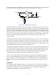
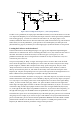
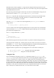
I/O
1k
1k
74xx244input output
Raspi
1k
10k
3.3V
Figure 9: The circuit diagram for I/O ports 1, 2, and 3 (with pushbutton).
In order to use a pushbutton, the input jumper must not be installed, even if the intention is to use this
as an input to the Raspberry Pi. If it is installed, the output of the lower buffer prevents the pushbutton
from working properly. To make clear what state each button is in, the output jumper can be
installed, and then the LED will now show the button state (LED on means button up, LED off means
button down). To use the pushbuttons, a pull-up must be set on the Raspberry Pi GPIO pins used
(described below, page 19) so that they are read as high (logical 1) when the buttons are not pressed.
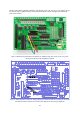
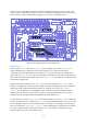
Locating the I/O Ports on the Gertboard
In the functional blocks location diagram (Figure 2 on page 6), the components implementing the
buffered I/O are outlined in red. The ICs containing the buffers are U3, U4, and U5 near the centre of
the board. The LEDs are labelled D1 to D12; D1 is driven by port 1, D2 by port 2, etc. The
pushbutton switches (the silver rectangular devices with black circles) are labelled S1 to S3; S1 is
connected to port 1 and so on.
The pins corresponding to „Raspi‟ in Figure 8 and Figure 9 above are B1 to B12 on the J3 header
above and to the right of the words „Raspberry Pi‟ on the board (B1 to B3 correspond to the „Raspi‟
points in Figure 9, and B4 to B12 correspond to the „Raspi‟ points in Figure 8). They are called
„Raspi‟ because these are the ones that are usually connected to the pins in header J2, which are
directly connected to the pins in J1, and which are then finally connected to the GPIO pins on the
Raspberry Pi. The pins corresponding to the „I/O‟ point on the right of the circuit diagrams above are
BUF1 to BUF12 in the (unlabeled) single row header at the top of the Gertboard.
On the Gertboard schematic, I/O buffers are on page A-2. The buffer chips U3, U4, and U5 are clearly
labelled. It should be clear that ports 1 to 4 are handled by chip U3, ports 5 to 8 by chip U4, and ports
9 to 12 by chip U5. The „Raspi‟ points in the circuit diagrams above are shown as the signals BUF_1
to BUF_12 on the left side of the page, and the „I/O‟ points are BUF1 to BUF12 to the right of the
buffer chips. The input jumper locations are the blue rectangles labelled P1, P3, P5, P7, etc to the left
of the buffer chips, and the output jumper locations are the blue rectangles labelled P2, P4, P6, P8,
etc, to the right of the buffer chips. The pushbutton switches S1, S2, and S3 are shown separately, on
the right side of the page near the middle. Below the pushbuttons, the pull-up resistors are shown.
The buffered I/O ports can be used with (almost) any of the GPIO pins; they just have to be connected
using straps. So for example, if you want to use port 1 with GPIO17 a strap is placed between the B1
pin in J3 and the GP17 pin in J2. Beware that the pushbuttons cannot be used with GPIO0 or GPIO1
(GP0 and GP1 in header J2 on the board) as those two pins have a 1800Ω pull-up resistor on the
Raspberry Pi. When the button is pressed the voltage on the input will be