FEN LOGIC LTD. Gertboard User Manual Gert van Loo and Myra VanInwegen Revision 2.0 The Gertboard is an add-on GPIO expansion board for the Raspberry Pi computer. It comes with a large variety of components, including buttons, LEDs, A/D and D/A converters, a motor controller, and an Atmel AVR microcontroller. There are test programs for the Gertboard written in C and Python, which are freely available on the Web.
Contents Gertboard Overview................................................................................................................................ 5 Labels and Diagrams........................................................................................................................... 7 Power on the Gertboard ...................................................................................................................... 9 GPIO Pins .......................................................
D/A and A/D tests in C ................................................................................................................. 35 D/A and A/D tests in Python......................................................................................................... 36 Combined Tests .................................................................................................................................... 38 A/D and Motor Controller ............................................................
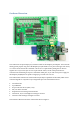
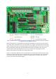
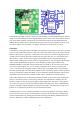
Gertboard Overview Figure 1: Gertboard and Raspberry Pi The Gertboard is an input/output (I/O) extension board for the Raspberry Pi computer. It fits onto the GPIO (general purpose I/O) pins of the Raspberry Pi (the double row of pins on the upper left corner) via a socket on the back of the Gertboard. A bit of care is required when putting the two devices together. It is easy to insert just one row of pins into the socket, but all of the pins need to be connected.
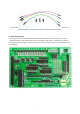
Figure 2: Functional blocks diagram: the key blocks are identified by coloured boundary marking. Please note that the appearance of some components can vary. This annotated photo of a populated (fully assembled) Gertboard shows where the functional blocks are located. Some of the blocks have two areas marked.
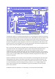
Figure 3: Photograph showing straps (the coloured wires) above, and jumpers below. Straps connect two parts of Gertboard together, whilst jumpers conveniently connect two adjacent pins together. Labels and Diagrams As you get to know the Gertboard and make connections between the various blocks, you will be guided extensively by the white labels on the circuit board.
Figure 5: Diagram representing a bare Gertboard circuit board. The blue elements correspond to the white lines and text, and the gray elements correspond to the silver coloured pads. The diagram in Figure 5 is created from the files that were used to design the Gertboard circuit board. The blue in the diagram is generated from the silkscreen file, which indicates where the white text and lines on the circuit board will be.
7 6 5 1 2 3 4 20 19 18 17 16 15 14 13 12 11 1 2 3 4 5 6 7 8 9 10 Figure 6: Two examples of ICs – an 8-pin and a 20-pin dual-inline package (DIP). In this package style, pin 1 is always identified as the first pin anticlockwise from the package notch marking. Integrated circuits (also known as ICs or chips), are marked Un.
Figure 7: Power jumper installed in header J7: photo on left, diagram on right The diagram on the right of Figure 7 above is our first example of a wiring diagram based on the blue and grey circuit board diagram. These diagrams indicate pins via black circles around the locations of pins on the board, and show connections as black lines between the circles. The diagram does not indicate directly whether the two pins should be joined by straps (wires) or jumpers.
Label on GB Port on RPi1 Port on RPi2 Alt function (which alt) Purpose GP0 GPIO0 GPIO2 SDA I2C bus GP1 GPIO1 GPIO3 SCL GP4 GPIO4 GPIO4 GP7 GPIO7 GPIO7 SPI_CE1_N (alt 0) GP8 GPIO8 GPIO8 SPI_CE0_N (alt 0) GP9 GPIO9 GPIO9 SPI_MISO (alt 0) SPI bus GP10 GPIO10 GPIO10 SPI_MOSI (alt 0) GP11 GPIO11 GPIO11 SPI_SCLK (alt 0) GP14 GPIO14 GPIO14 TXD0 (alt 0) UART GP15 GPIO15 GPIO15 RXD0 (alt 0) GP17 GPIO17 GPIO17 GP18 GPIO18 GPIO18 PWM0 (alt 5) pulse width modulation GP21 GPIO21 GPIO27 GP22 GPIO22 GPIO22 GP23 GPIO23 GPI
To retrieve the original software, put the file where you want your Gertboard software to end up on your Raspberry Pi computer, then extract the files by typing the following in one of the terminal windows on your RPi (substituting the name of the actual file you have downloaded for the file name we are using in this example): unzip gertboard_sw_20120725.zip A new directory, gertboard_sw, will be created. Change to this directory (by typing cd gertboard_sw) and list the contents (ls).
Macro name T Explanation INP_GPIO(n) E activates GPIO pin number n (for input) OUT_GPIO(n) E used after above, sets pin n for output SET_GPIO_ALT(n, a) E used after INP_GPIO, select alternate function for pin GPIO_PULL W set pull code GPIO_PULLCCLK0 W select which pins pull code is applied to GPIO_IN0 R get input values GPIO_SET0 W select which pins are set high GPIO_CLR0 W select which pins are set low Page no.
unzip GB_Python.zip cd GB_Python ls The ls lists all the files in the directory. Most of them end in .py and are Python programs. The file README.txt contains (amongst other info) instructions on how to install the packages you need to run the Python programs. Once you have the necessary packages installed, you can run the programs. For example, if want to run the program leds-rg.py, which tests the LEDs (using the RPi.GPIO package, see below) type: sudo python leds-rg.
output from the RPi. It is important to keep this in mind as the Gertboard is set up: an output from the Gertboard is an input to the Raspberry Pi, and so the input jumper must be installed. Raspi 3.3V input 74xx244 output 1k 10k I/O 1k Figure 8: The circuit diagram for I/O ports 4-12. The triangle symbols in the diagram above represent buffers; they propagate logical values (low and high) in the direction the triangle is pointing.
Raspi 3.3V input 1k 74xx244 output 10k 1k I/O 1k Figure 9: The circuit diagram for I/O ports 1, 2, and 3 (with pushbutton). In order to use a pushbutton, the input jumper must not be installed, even if the intention is to use this as an input to the Raspberry Pi. If it is installed, the output of the lower buffer prevents the pushbutton from working properly.
This is not an I/O voltage which can be reliably seen as low. The output and input jumper locations are above and below the U3, U4, and U5 buffer chips. The input jumpers need to be placed on the headers below the chips (shown on the board with the „in‟ text; they are separated from the chip they go with by four small resistors), and the „output‟ jumpers need to be placed on the headers above the chips (with the „out‟ text).
GPIO23 will read the rightmost pushbutton. The jumpers on the „out‟ area of U3 (U3-out-B1, U3-outB2, U3-out-B3) are optional: if they are installed, the leftmost 3 LEDs will light up to indicate the state of the switches. Figure 11: Photo showing connections for the buttons test. Whilst the image above is clear, it isn’t very good at showing exactly how the straps and jumpers are placed. Figure 12: Wiring diagram for buttons test.
In the diagram in Figure 12, black circles show which pins are being connected, and black lines between two pins indicate that jumpers (if they are adjacent) or straps (if they are further apart) are used to connect them. Buttons Test in C The code specific to the buttons test is buttons.c. In the main routine, the connections required for this test are firstly printed to the terminal (a text description of the wiring diagram above).
Note that because of the way Python for loops work, the end point of the loop must be set to one beyond the last item in the range that you want to cover. So in order to set port 25, the end point of the loop command must be set to 26. Next, the wiring instructions appear on the screen. Once the user confirms that the wiring is ok, the initial values for variables button_press and previous_status are set. Next a while loop runs until 19 button presses/releases have occurred.
If there aren‟t enough jumpers or straps to wire these connections all up at once, don‟t worry. Just wire up as many as possible and run the test. Once it‟s finished the straps/jumpers can be moved and the test can be run again. Nothing bad will happen if you write to an unconnected pin. Figure 13: The wiring diagram for the LED test program LEDs Test in C The test code in leds.c first calls setup_io to get everything ready.
The test program flashes the LEDs in three patterns. The patterns are specified by a collection of global arrays given values using an initializer. The number in each of the arrays says which LEDs will be turned on at that point in the pattern – so, pattern value is submitted sequentially to produce the changing pattern, switching all the LEDs off between successive pattern values. Each pattern is run through twice. The first pattern lights the LEDs one at a time in sequence, left to right.
Testing I/O Our two examples so far have only used the ports to access the pushbuttons and LEDs. The next example, called butled (for BUTton LED) in C, or butled-rg.py (in Python), will show one of the ports serving just as an input port. The idea is that one port (along with its button) is used to generate a signal, and software then sends that signal to another port which it is used as just an input. We read both ports in and print them on the screen.
Butled Test in C In butled.c we use INP_GPIO to set GPIO22 and GPIO23 to input and GPIO_PULL and GPIO_PULLCLK0 to set the pull-up on GPIO23. This is described in more detail on page 19, in the buttons test. Then the GPIO values are repeatedly read in, and the binary values of GPIO22 and GPIO23 are printed out (with GPIO23 first), if they have changed since the last cycle. So if „01‟ is displayed on the monitor, we can see that GPIO23 is low and GPIO22 is high.
common OUT Raspi Figure 15: Circuit diagram of each open collector driver. The „common‟ pin is, as the name states, common for all open collector drivers. It is not connected to anything else on the Gertboard. As with all devices the control for the open collector drivers (the „Raspi‟ point) can also be connected to the ATmega controller to, for example, drive relays or motors. The open collector drivers are in the schematics on page A-3.
Now, when RLY1 in J4 is set low, the circuit doesn‟t receive any power and thus is off. When RLY1 in J4 goes high, the open collector driver uses transistors to connect the „ground‟ side of the circuit to the ground on the board, and since this is connected to the ground terminal on the power supply, the power supply powers your circuit: it is just turned off and on by the open collector driver. Figure 16: Wiring diagram to test the open collector drivers.
ten times with a 0.4 second delay between each change. At the end, or on (CTRL-C) keyboard interrupt, the GPIO ports are reset. Suggested safe tweaks to experiment with. Try changing these one at a time and see what they do... vary the 0.4 in sleep(0.
1 0 Figure 17: An example of a PWM output. Here the output is on for 50% of the time, so it has a duty cycle of 50%. With a PWM, you can control the amount of time the output is high vs. when it is low. This is called the duty cycle and is expressed as a percentage. Figure 17 above shows a 50% duty cycle; the one in Figure 18 below is 25%. 1 0 Figure 18: In this PWM example, the duty cycle is 25%.
Figure 21: The wiring diagram for the test program motor. Motor Test in C The PWM is controlled by a memory map, like the GPIO and SPI bus. This memory map is part of the setup_io function in gb_common.c, so that is whether the PWM is used or not. Further setup code is found in, gb_pwm.c, with an associated header file gb_pwm.h. The function setup_pwm in gb_pwm.
details about alternative functions of the GPIO pins. For a summary of the alternate function of GPIO pins used on the Gertboard, see Table 1 on page 11.) We set the output of GPIO17 low (to make sure that the motor doesn‟t turn) and then initialize the PWM by calling setup_pwm. We enable the PWM by setting the mode to PWM0_ENABLE using force_pwm0.
repetitions is just one step up or down in motor speed: 400 repetitions at 2000 Hertz represents just 0.2 seconds. Then we define the run_loop() function run_loop(startloop, endloop, step, port_num, printchar) The arguments startloop and endloop are the % time for the switched port to be ON at the start and end of the loop. step is the size of the increment for each successive loop. port_num is the port we‟re switching (17 or 18).
with. step is the incremental/decremental PWM value for each successive loop. printchar is the character to denote motor accelerating or decelerating. The main body of the program contains four calls to loop() to demonstrate acceleration and deceleration in each of two different rotational directions, with a short “aesthetic” pause in between each loop, defined by rest = 0.013 (0.013s). When port 17 is 0, the motor rotates in one direction. When port 17 is 1, it rotates the other way.
assumes that writes are in 12 bits, so it is important that the value is selected appropriately (details are below in the section “Testing the D/A and A/D”). The maximum output voltage of the D/A – the output voltage when you send an input of all 1s – is 2.04V. The analogue outputs of the two channels go to pins labelled DA0 (for channel 0) and DA1 (for channel 1) in the J29 header on the left edge of the board. Just next to these pins are ground pins (GND) to provide a reference.
The red lead needs to be connected to DA0 (to test the D/A channel 0 which is shown below) or DA1 (for channel 1). Switch the multimeter on, and set it to measure voltages from 0 to around 5V. All this is shown in Figure 22. The C test program for the A/D is called atod; the Python version is atod.py. To run this test a voltage source on the analogue input is required. This is most easily provided by a potentiometer (a variable resistor). The two ends of the potentiometer are connected, one side to high (3.
Figure 24: The wiring diagram for the dad test, which allows you to test the A/D and D/A converters together, without the aid of a multimeter or potentiometer. D/A and A/D tests in C Since the D/A and A/D converters both use the SPI bus, the common SPI bus code has been placed into a separate file, gb_spi.c. There is also an associated header file, gb_spi.h, which contains many macros and constants needed for interacting with the SPI bus, as well as the declarations for the functions in gb_spi.c.
use, then calls setup_gpio to choose which pins to use and how to use them. In setup_gpio, as usual INP_GPIO(n) (where n is the pin number) is used to activate the pins. This also sets them up to be used as inputs. They should however, be used as an SPI bus, which is one of the alternative functions for these pins (it is alternate 0). Thus we use SET_GPIO_ALT(n, a) (where n is the pin number and a is the alternate number, in this case 0) to select this alternate use of the pins.
potentiometer. It uses the display(char, reps, adc_value, spaces) function to achieve this. Moving the potentiometer while the program is running changes both the numerical readout and the number of # characters displayed. Suggested tweaks to experiment with. Try changing these one at a time and see what they do... char = '#' – change value of char from # to a symbol of your choice (line 30) sleep(0.05) – change the 0.05 and see what happens (line 56) dtoa.
Change the 4 in adc_string = "{0:04d}" Change the 3 in print "%s %s %s" % ("{0:03d}") Remove the jumper between AD0 and DA1 and see what happens Combined Tests This section shows some examples of using more than one functional block at a time. A/D and Motor Controller In the potmot (for potentiometer-motor) test we use a potentiometer (“pot”) connected to the analogue to digital converter (A/D) to get an input value, and this value is used to control the speed and direction of the motor.
Potmot Test in C The main routine for this is in potmot.c. Functions from gb_spi.c and gb_pwm.c are used to control the SPI bus (for reading the A/D) and the pulse width modulator (for controlling the speed of the motor). In the main routine for potmot, first we print to the terminal the connections that need to be made on the Gertboard to run this example, then we call setup_io to set up the GPIO ready for use. Then we call setup_gpio to set the GPIO pins the way we want them.
The main loop is wrapped in a try: except: block to enable safe resetting of the ports in the event of a CTRL+C keyboard interrupt. Suggested safe tweaks to experiment with. none this time Decoder The decoder implemented by the decoder program takes the three pushbuttons as input and turns on one of 8 LEDs to indicate the number with the binary encoding given by the state of the buttons. Switch S1 gives the most significant bit of the number, S2 the middle bit, and S3 the least significant bit.
selecting them for input and enabling a pull-up, as described on page 19) and to set GPIO11 to GP7, GPIO4, GPIO1, and GPIO0 up as outputs (as described on page 13). Then we enter a loop where we read the state of the pushbuttons and light up the LED corresponding to this number (after turning off the LED previously set). We turn the LEDs on and off using GPIO_SET0 and GPIO_CLR0 as described on page 21. At the time of writing, there is no decoder test in Python.
options for the ATmega168 and ATmega328, the ones most commonly used on the Gertboard). Then go to the Tools > Programmer menu and choose “Raspberry Pi GPIO”. Arduino Pins on the Gertboard All the input and output pins of the ATmega chip are brought out to header J25 on the left edge of the board. They are labelled PCn, PDn, and PBn, where n is a number. These labels correspond to the pinout diagrams of the ATmega168/328 chips.
Uploading Sketches using the SPI Bus In order to get your sketch running on the ATmega chip on the Gertboard, it has to be transferred over to the chip somehow (this is called uploading the sketch). There are various methods used to program ATmega chips, but we are going to use the SPI bus available on GPIO pins 8 through 11. This is possible because your Arduino IDE is using the special downloader/uploader (avrdude) that you got from projects.drogon.net.
Figure 28: Wiring diagram for the sketch Blink. Note that in this diagram we have not shown the connections to the SPI pins. Once you have uploaded the code, you no longer need them and can remove the straps. On the other hand, if you want you can leave them in place, and this is a good idea if you are planning on uploading some other sketches later. Button Sketch Let‟s look at another fairly simple sketch called Button, located under File > Examples > Digital menu in both 0018 and 1.0.1.
Figure 30: Circuit in use on the Gertboard, showing an additional 1k resistor to protect the input to BCM2835. The 1K resistor between the pushbutton and the „Raspi‟ point is to protect the BCM2835 (the processor on the Raspberry Pi) if you accidentally set the GPIO pin connected to „Raspi‟ to output instead of input.
Figure 31: Wiring diagram for the sketch Button. When you have done this, the first LED will be on when the third button is pressed, and off when the third button is up. AnalogInput Sketch Now let‟s try using an analogue pin. Find the AnalogInput sketch under File > Examples > Analog. This reads in a value from analogue input 0 (which has already been converted by the internal A/D to a value between 0 and 1023), then uses that number as a delay between turning an LED on and off.
Figure 32: Wiring diagram for the AnalogInput sketch. AnalogReadSerial Sketch Using Minicom Some of the Arduino sketches involve reading or writing data via the serial port, or UART. An example is AnalogReadSerial which is in File > Examples > Basics. This sketch sets the baud rate to 9600, then repeatedly reads in a value from analogue pin 0 and prints this value to the serial port (also called UART).
Figure 33: Wiring diagram for the sketch AnalogReadSerial. GPIO14 and GPIO15 are the pins that the Raspberry Pi uses for the UART serial port. If you refer back to the table of alternate functions (Table 1, page 11), you will see that GPIO14 is listed as TX and GPIO15 as RX. This is not a mistake! This swapping is necessary: the data that is transmitted by the ATmega is received by the Raspberry Pi, and vice versa.
showing the voltage from an analogue input such as a potentiometer. First you need to put this sketch in the right place. You should have a directory called sketchbook in your home directory. Make a subdirectory beneath that called LEDmeter, and copy LEDmeter.ino into that directory. To do this, you can type the following from your gertboard_sw directory: mkdir ~/sketchbook/LEDmeter cp LEDmeter.
Going Forward These examples have only just scratched the surface of the wonderful world of Arduino. Check out http://arduino.cc/en/Tutorial/HomePage for much, much more. For More Information For further information on the Raspberry Pi and its GPIO ports, the datasheet for the processor can be found here: http://www.raspberrypi.org/wp-content/uploads/2012/02/BCM2835-ARM-Peripherals.pdf Appendix A: Schematics We have included the schematics for the Gertboard in the pages that follow.
51