
Datasheet

11 | Page
5 Connectors
The board contains a number of connectors. You will find that in the document the connectors of
the Atmega devices have two ways of numbering: There are the single numbers 0..13 and
A1..A3. These are the numbers used in many Arduino example programs. Alongside those I use
the official pin names (PB0..PB7, PD0..PD7, PCO..PC3). The latter are easier to use if you have
to work with the AVR datasheet.
5.1 Alternate functions.
The Atmega-328 and the Atemege-48 have exactly the same pins with the same functionality.
The devices only differ in the size of their various memories. The following is a table of the pins
and all the functions they can carry. These where copied from the AVR datasheet. For details of
the functions you should read that datasheet.
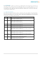
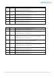
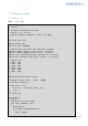
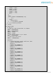
#
Name
Functions
-
PB7
XTAL2 (Chip Clock Oscillator pin 2)
TOSC2 (Timer Oscillator pin 2)
PCINT7 (Pin Change Interrupt 7)
-
PB6
XTAL1 (Chip Clock Oscillator pin 1 or External clock input)
TOSC1 (Timer Oscillator pin 1)
PCINT6 (Pin Change Interrupt 6)
13
PB5
SCK (SPI Bus Master clock Input)
PCINT5 (Pin Change Interrupt 5)
12
PB4
MISO (SPI Bus Master Input/Slave Output)
PCINT4 (Pin Change Interrupt 4)
11
PB3
MOSI (SPI Bus Master Output/Slave Input)
OC2A (Timer/Counter2 Output Compare Match A Output)
PCINT3 (Pin Change Interrupt 3)
10
PB2
SS (SPI Bus Master Slave select)
OC1B (Timer/Counter1 Output Compare Match B Output)
PCINT2 (Pin Change Interrupt 2)
9
PB1
OC1A (Timer/Counter1 Output Compare Match A Output)
PCINT1 (Pin Change Interrupt 1)
8
PB0
ICP1 (Timer/Counter1 Input Capture Input)
CLKO (Divided System Clock Output)
PCINT0 (Pin Change Interrupt 0)