
Datasheet

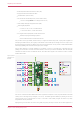

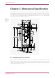
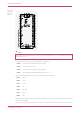
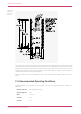
Table Of Contents

SMPS to generate the 3.3V for the RP2040 and its GPIO.
3V3_EN connects to the on-board SMPS enable pin, and is pulled high (to VSYS) via a 100K resistor. To disable the 3.3V
(which also de-powers the RP2040), short this pin low.
3V3 is the main 3.3V supply to RP2040 and its I/O, generated by the on-board SMPS. This pin can be used to power
external circuitry (maximum output current will depend on RP2040 load and VSYS voltage, it is recommended to keep the
load on this pin less than 300mA).
ADC_VREF is the ADC power supply (and reference) voltage, and is generated on Pico by filtering the 3.3V supply. This pin
can be used with an external reference if better ADC performance is required.
AGND is the ground reference for GPIO26-29, there is a separate analog ground plane running under these signals and
terminating at this pin. If the ADC is not used or ADC performance is not critical, this pin can be connected to digital
ground.
RUN is the RP2040 enable pin, and has an internal (on-chip) pull-up resistor to 3.3V of about ~50K Ohms. To reset
RP2040, short this pin low.
Finally, there are also 6 Test Points (TP1-TP6) which can be accessed if required, for example if using as a surface mount
module. These are:
TP1 Ground (close coupled ground for differential USB signals)
TP2 USB DM
TP3 USB DP
TP4 GPIO23/SMPS PS pin (do not use)
TP5 GPIO25/LED (not recommended to be used)
TP6 BOOTSEL
TP1, TP2 and TP3 can be used to access the USB signals instead of using the micro-USB port. TP6 can be used to drive
the system into mass-storage USB programming mode (by shorting it low at power-up). Note that TP4 is not intended to
be used externally, and TP5 is not really recommended to be used as it will only swing from 0V to the LED forward voltage
(and hence can only really be used as an output with special care).
2.2. Surface Mount Footprint
The following footprint (Figure 5) is recommended for systems which will be reflow-soldering Pico units as modules.
Raspberry Pi Pico Datasheet
2.2. Surface Mount Footprint 8