
Datasheet

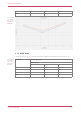
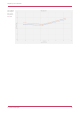
Table Of Contents
For much improved ADC performance, an external 3.0V shunt reference, such as LM4040, can be connected from the
ADC_VREF pin to ground. Note that if doing this the ADC range is limited to 0-3.0V signals (rather than 0-3.3V), and the
shunt reference will draw continuous current through the 200R filter resistor (3.3V-3.0V)/200 = ~1.5mA.
Note that the 1R resistor on Pico (R9) is designed to (maybe) help with shunt references that would otherwise become
unstable when directly connected to 2.2μF. It also makes sure there is a little filtering even in the case that 3.3V and
ADC_VREF are shorted together (which is a valid thing to do if you don’t care about noise and want to reduce the inherent
offset).
Finally, R7 is a physically large 1608 metric (0603) package resistor, so can be relatively easily removed if a user wants to
isolate ADC_VREF and do their own thing with the ADC voltage, for example powering it from an entirely separate voltage
(e.g. 2.5V). Note that the ADC on RP2040 has only been qualified at 3.0/3.3V but should work down to about 2V.
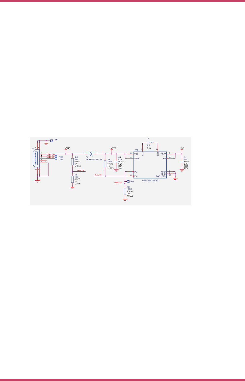
4.4. Powerchain
Raspberry Pi Pico has been designed with a simple yet flexible power supply architecture and can easily be powered from
other sources such as batteries or external supplies. Integrating the Pico with external charging circuits is also
straightforward. Figure 14 shows the power supply circuitry.
Figure 14. The
powerchain of the
Raspberry Pi Pico
Rev3 board.
VBUS is the 5V input from the micro-USB port, which is fed through a Schottky diode to generate VSYS. The VBUS to
VSYS diode (D1) adds flexibility by allowing power ORing of different supplies into VSYS.
VSYS is the main system 'input voltage' and feeds the RT6150 buck-boost SMPS, which generates a fixed 3.3V output for
the RP2040 device and its IO (and can be used to power external circuitry). VSYS is R-C filtered and divided by 3 (by R5, R6
and C3 in the Pico schematic) and can be monitored on ADC channel 3. This can be used for example as a crude battery
voltage monitor.
The buck-boost SMPS, as its name implies, can seamlessly switch from buck to boost mode, and therefore can maintain
an output voltage of 3.3V from a wide range of input voltages, ~1.8V to 5.5V, which allows a lot of flexibility in the choice
of power source.
GPIO24 monitors the existence of VBUS, while R10 and R1 act to pull VBUS down to make sure it is 0V if VBUS is not
present.
GPIO23 controls the RT6150 PS (Power Save) pin. When PS is low (the default on Pico) the regulator is in Pulse
Frequency Modulation mode, which, at light loads, saves considerable power by only turning on the switching MOSFETs
occasionally to keep the output capacitor topped up. Setting PS high forces the regulator into Pulse Width Modulation
(PWM) mode. PWM mode forces the SMPS to switch continuously, which reduces the output ripple considerably at light
loads (which can be good for some use cases) but at the expense of much worse efficiency. Note that under heavy load
the switcher will be in PWM mode irrespective of the PS pin state.
The SMPS EN pin is pulled up to VSYS by a 100K resistor and made available on Pico pin 37. Shorting this pin to ground
will disable the switcher and put it into a low power state.
Raspberry Pi Pico Datasheet
4.4. Powerchain 18