
Datasheet

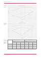
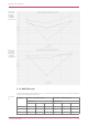
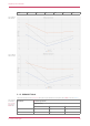
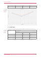

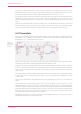
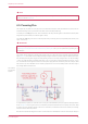
Table Of Contents

Chapter 4. Applications Information
4.1. Programming the Flash
The on-board 2MByte QSPI Flash can be (re)programmed either using the Serial Wire Debug port or by the special USB
Mass Storage Device mode.
The simplest way to reprogram the Pico’s Flash is to use the USB mode. To do this, depower the board, then hold the
BOOTSEL button down during board power-up (e.g. hold BOOTSEL down while connecting the USB). The Pico will then
appear as a USB Mass Storage Device. Dragging a special '.uf2' file onto the disk will write this file to the Flash and restart
the Pico.
The USB boot code is stored in ROM on RP2040, so can not be accidentally overwritten.
To get started using the SWD port see the Debugging with SWD section in the Getting started with Raspberry Pi Pico
book.
4.2. General Purpose IO
The Raspberry Pi Pico’s GPIO is powered from the on-board 3.3V rail and is therefore fixed at 3.3V.
The Pico exposes 26 of the 30 possible RP2040 GPIO pins by routing them straight out to Pico header pins. GPIO0 to
GPIO22 are digital only and GPIO 26-28 are able to be used either as digital GPIO or as ADC inputs (software selectable).
One thing to note is that the ADC capable GPIO26-29 have an internal reverse diode to the VDDIO (3V3) rail and so the
input voltage must not exceed VDDIO plus about 300mV. Also, if the RP2040 is unpowered, applying a voltage to these
GPIO pins will 'leak' through the diode into the VDDIO rail. Normal digital GPIO pins 0-25 (and also the debug pins) do not
have this restriction and therefore voltage can safely be applied to these pins when RP2040 is upowered.
4.3. Using the ADC
The RP2040 ADC does not have an on-board reference and therefore uses its own power supply as a reference. On Pico
the ADC_AVDD pin (the ADC supply) is generated from the SMPS 3.3V by using an R-C filter (201 ohms into 2.2μF). This is
a simple solution but does have the following drawbacks:
1. We are relying on the 3.3V SMPS output accuracy which isn’t great
2. We can only do so much filtering and therefore ADC_AVDD will be somewhat noisy
3. The ADC draws current (about 150μA if the temperature sense diode is disabled, but it varies from chip to chip) and
therefore there will be an inherent offset of about 150μA*200 = ~30mV. There is a small difference in current draw
when the ADC is sampling (about +20μA) so that offset will also vary with sampling as well as operating
temperature.
Changing the resistance between the ADC_VREF and 3V3 pin can reduce the offset at the expense of more noise - which
may be OK especially if the use case can support averaging over multiple samples.
Driving high the SMPS mode pin (GPIO23), to force the power supply into PWM mode, can greatly reduce the inherent
ripple of the SMPS at light load, and therefore the ripple on the ADC supply. This does reduce the power efficiency of the
board at light load, so the low-power PFM mode can be re-enabled between infrequent ADC measurements by driving
GPIO23 low once more. See Section 4.4.
The ADC offset can be reduced by tying a second channel of the ADC to ground, and using this zero-measurement as an
approximation to the offset.
Raspberry Pi Pico Datasheet
4.1. Programming the Flash 17