Communications Radio User Manual
Manuals
Brands
Ranger Manuals
Radio
RCI-6300F TB
11
12
13
14
15
16
17
18
19
20
- 19 -
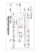
Figure 4-3 Main PCB Adjustment Location
1
...
...
18
19
20
21
22
...
...
45