
Manual


Preliminary W49L102
Publication Release Date: June 1999
- 11 - Revision A1
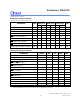
DC CHARACTERISTICS
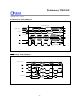
Absolute Maximum Ratings
PARAMETER RATING UNIT
Power Supply Voltage to Vss Potential -0.5 to +4.6 V
Operating Temperature 0 to +70
°C
Storage Temperature -65 to +150
°C
D.C. Voltage on Any Pin to Ground Potential except A9 -0.5 to VDD +1.0 V
Transient Voltage (<20 nS ) on Any Pin to Ground Potential -1.0 to VDD +1.0 V
Voltage on A9 Pin to Ground Potential -0.5 to 12.5 V
Note: Exposure to conditions beyond those listed under Absolute Maximum Ratings may adversely affect the life and reliability of the
device.
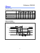
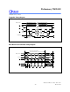
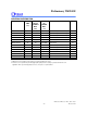
DC Operating Characteristics
(VDD = 3.3V ± 0.3V, VSS = 0V, TA = 0 to 70° C)
PARAMETER SYM. TEST CONDITIONS LIMITS UNIT
MIN. TYP. MAX.
Power Supply
Current
ICC
CE
=
OE
= VIL,
WE
= VIH, all I/Os open
Address inputs = VIL/VIH, at f = 5 MHz
- 15 25 mA
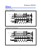
Standby VDD
Current (TTL input)
ISB1
CE
= VIH, all I/Os open
Other inputs = VIL/VIH
- - 1 mA
Standby VDD
Current
(CMOS input)
ISB2
CE
= VDD -0.3V, all I/Os open
Other inputs = VDD -0.3V/GND
- 10 50
µA
Input Leakage
Current
ILI VIN = GND to VDD - - 10
µA
Output Leakage
Current
ILO VOUT = GND to VDD - - 10
µA
Input Low Voltage VIL - -0.3 - 0.6 V
Input High Voltage VIH - 2.0 - VDD +0.5 V
Output Low Voltage VOL IOL = 1.6 mA - - 0.45 V
Output High Voltage VOH IOH = -0.1 mA 2.4 - - V