
Owner's manual

W49F002U
- 14 -
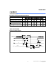
AC Characteristics, continued
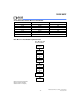
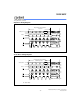
Read Cycle Timing Parameters
(VCC = 5.0V
±
10
%
, VCC = 0V, TA = 0 to 70
°
C)
PARAMETER SYM.
W49F002U-70
W49F002U-90
W49F002U-120
UNIT
MIN. MAX.
MIN. MAX.
MIN. MAX.
Read Cycle Time T
RC
70 - 90 - 120 - nS
Chip Enable Access Time T
CE
- 70 - 90 - 120 nS
Address Access Time T
AA
- 70 - 90 - 120 nS
Output Enable Access Time T
OE
- 35 - 40 - 50 nS
CE Low to Active Output
T
CLZ
0 - 0 - 0 - nS
OE Low to Active Output
T
OLZ
0 - 0 - 0 - nS
CE
High to High-Z Output
T
CHZ
- 25 - 25 - 30 nS
OE
High to High-Z Output
T
OHZ
- 25 - 25 - 30 nS
Output Hold from Address Change T
OH
0 - 0 - 0 - nS
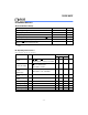
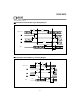
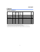
Write Cycle Timing Parameters
PARAMETER SYMBOL MIN. TYP. MAX. UNIT
Address Setup Time T
AS
0 - - nS
Address Hold Time T
AH
50 - - nS
WE
and
CE Setup Time
T
CS
0 - - nS
WE
and
CE Hold Time
T
CH
0 - - nS
OE
High Setup Time
T
OES
0 - - nS
OE High Hold Time
T
OEH
0 - - nS
CE Pulse Width
T
CP
100 - - nS
WE
Pulse Width
T
WP
100 - - nS
WE
High Width
T
WPH
100 - - nS
Data Setup Time T
DS
50 - - nS
Data Hold Time T
DH
10 - - nS
Byte Programming Time T
BP
- 35 50
µS
Erase Cycle Time T
EC
- 0.1 0.2 S
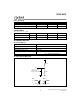
Note: All AC timing signals observe the following guidelines for determining setup and hold times:
(a) High level signal's reference level is V
IH
and (b) low level signal's reference level is V
IL
.