
Owner's manual

W49F002U
Publication Release Date: April 2000
- 13 - Revision A2
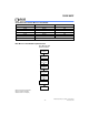
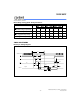
Power-up Timing
PARAMETER SYMBOL TYPICAL UNIT
Power-up to Read Operation T
PU
. READ 100
µ
S
Power-up to Write Operation T
PU
. WRITE 5 mS
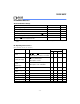
CAPACITANCE
(VDD = 5.0V, TA = 25
°
C, f = 1 MHz)
PARAMETER SYMBOL CONDITIONS MAX. UNIT
I/O Pin Capacitance C
I/O
V
I/O
= 0V 12 pf
Input Capacitance C
IN
V
IN
= 0V 6 pf
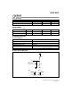
AC CHARACTERISTICS
AC Test Conditions
PARAMETER CONDITIONS
Input Pulse Levels 0V to 3.0V
Input Rise/Fall Time < 5 nS
Input/Output Timing Level 1.5V/1.5V
Output Load 1 TTL Gate and C
L
= 100 pF for 120 nS;
C
L
= 30 pF for 70 nS /90 nS
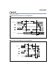
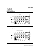
AC Test Load and Waveform
+5V
1.8K
1.3K
D
OUT
Ω
Ω
30 pF for 70nS / 90nS
(Including Jig and Scope)
Input
3V
0V
Test Point
Test Point
1.5V
1.5V
Output
100 pF for 120nS