
Owner manual


W29EE512
Publication Release Date: April 2000
- 11 - Revision A6
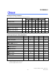
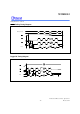
Read Cycle Timing Parameters
(V
CC
= 5.0V
±
10
%
, V
CC
= 5.0
±
5
%
for 70 nS, V
SS
= 0V, T
A
= 0 to 70
°
C)
PARAMETER SYM. W29EE512-70
W29EE512-90
W29EE512-12
UNIT
MIN. MAX.
MIN. MAX.
MIN. MAX.
Read Cycle Time T
RC
70 - 90 - 120 - nS
Chip Enable Access Time T
CE
- 70 - 90 - 120 nS
Address Access Time T
AA
- 70 - 90 - 120 nS
Output Enable Access Time T
OE
- 35 - 40 - 50 nS
CE
High to High-Z Output
T
CHZ
- 25 - 25 - 30 nS
OE
High to High-Z Output
T
OHZ
- 25 - 25 - 30 nS
Output Hold from Address Change T
OH
0 - 0 - 0 - nS
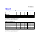
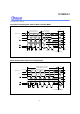
Byte/Page-write Cycle Timing Parameters
PARAMETER SYMBOL MIN. TYP. MAX. UNIT
Write Cycle (Erase and Program) T
WC
- - 10 mS
Address Setup Time T
AS
0 - - nS
Address Hold Time T
AH
50 - - nS
WE
and
CE
Setup Time
T
CS
0 - - nS
WE
and
CE
Hold Time
T
CH
0 - - nS
OE
High Setup Time
T
OES
0 - - nS
OE
High Hold Time
T
OEH
0 - - nS
CE
Pulse Width
T
CP
90 - - nS
WE
Pulse Width
T
WP
90 - - nS
WE
High Width
T
WPH
100 - - nS
Data Setup Time T
DS
35 - - nS
Data Hold Time T
DH
0 - - nS
Byte Load Cycle Time T
BLC
- - 200
µ
S
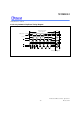
Notes: All AC timing signals observe the following guidelines for determining setup and hold times:
(1) High level signal's reference level is VIH.
(2) Low level signal's reference level is VIL.