
User Manual

W24512A
- 4 -
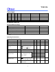
AC Characteristics, continued
(VDD = 5V ±10%, VSS = 0V, TA = 0 to 70° C)
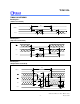
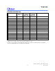
Read Cycle
PARAMETER SYM.
W24512A-15 W24512A-25 W24512A-25 W24512A-35
UNIT
MIN. MAX. MIN. MAX. MIN. MAX. MIN. MAX.
Read Cycle Time TRC 15 - 20 - 25 - 35 - nS
Address Access Time TAA - 15 - 20 - 25 - 35 nS
Chip Select Access Time
CS1
TACS1 - 15 - 20 - 25 - 35 nS
CS2 TACS2 - 15 - 20 - 25 - 35 nS
Output Enable to Output Valid TAOE - 7 - 10 - 12 - 17 nS
Chip Selection to Output in Low Z
CS1
TCLZ1* 3 - 3 - 3 - 3 - nS
CS2 TCLZ2* 3 - 3 - 3 - 3 - nS
Output Enable to Output in Low Z TOLZ* 0 - 0 - 0 - 0 - nS
Chip Deselection to Output in
CS1
TCHZ1* - 7 - 10 - 12 - 17 nS
High Z CS2 TCHZ2* - 7 - 10 - 12 - 17 nS
Output Disable to Output in High Z TOHZ* - 7 - 1 - 12 - 17 nS
Output Hold from Address Change TOH 3 - 3 - 3 - 3 - nS
* These parameters are sampled but not 100% tested.
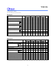
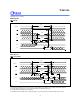
Write Cycle
PARAMETER SYM.
W24512A-15 W24512A-25 W24512A-25 W24512A-35
UNIT
MIN. MAX. MIN. MAX. MIN. MAX. MIN. MAX.
Write Cycle Time TWC 15 - 20 - 25 - 35 - nS
Chip Selection to End of Write
CS1
TCW1 13 - 17 - 18 - 20 - nS
CS2 TCW2 13 - 17 - 18 - 20 - nS
Address Valid to End of Write TAW 13 - 17 - 18 - 20 - nS
Address Setup Time TAS 0 - 0 - 0 - 0 - nS
Write Pulse Width TWP 10 - 12 - 15 - 18 - nS
Write Recovery Time
CS1
, WE
TWR1 0 - 0 - 0 - 0 - nS
CS2 TWR2 0 - 0 - 0 - 0 - nS
Data Valid to End of Write TDW 9 - 10 - 12 - 15 - nS
Data Hold from End of Write TDH 0 - 0 - 0 - 0 - nS
Write to Output in High Z TWHZ* - 8 - 10 - 12 - 15 nS
Output Disable to Output in High Z TOHZ* - 8 - 10 - 12 - 15 nS
Output Active from End of Write TOW 0 - 0 - 0 - 0 - nS
* These parameters are sampled but not 100% tested.