
User Manual

W24512A
Publication Release Date: March 1999
- 3 - Revision A7
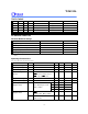
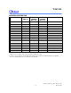
CAPACITANCE
(VDD = 5V, TA = 25° C, f = 1 MHz)
PARAMETER SYM. CONDITIONS MAX. UNIT
Input Capacitance CIN VIN = 0V 8 pF
Input/Output Capacitance CI/O VOUT = 0V 10 pF
Note: These parameters are sampled but not 100% tested.
THERMAL RESISTANCE
PARAMETER SYM. CONDITIONS MAX. UNIT
Junction to Case Thermal Resistance
θJC
A. F. R. = 1m/sec, TA = 25° C
20
°C/W
Junction to Ambient Thermal
Resistance
θJA
A. F. R. = 1m/sec, TA = 25° C
60
°C/W
Note: These parameters are only applied to "TSOP" and "SOJ" package types.
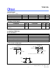
AC CHARACTERISTICS
AC Test Conditions
PARAMETER CONDITIONS
Input Pulse Levels 0V to 3V
Input Rise and Fall Times 5 nS
Input and Output Timing Reference Level 1.5V
Output Load CL = 30 pF, IOH/IOL = -4 mA/8 mA
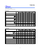
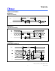
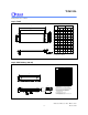
AC Test Loads and Waveform
90% 90%
5 nS
10%
5 nS
10%
R1 480 ohm
5V
OUTPUT
R2
255 ohm
30 pF
Including
Jig and
Scope
3.0V
0V
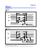
5V
OUTPUT
R1 480 ohm
5 pF
Including
Jig and
Scope
R2
255 ohm
(For T CLZ1,
CLZ2,
OLZ, CHZ1, CHZ2, OHZ,
WHZ,
OW
T
T
T
T T
T T
)