
User guide

Preliminary W24100
- 4 -
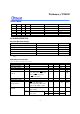
AC Characteristics, continued
(VDD = 5V
±
10%; VSS = 0V; TA = 0
°
C to 70
°
C)
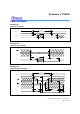
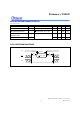
Read Cycle
PARAMETER SYM. W24100-70L W24100-70LL UNIT
MIN. MAX. MIN. MAX.
Read Cycle Time T
RC
70 - 70 - nS
Address Access Time T
AA
- 70 - 70 nS
Chip Select Access Time T
ACS
- 70 - 70 nS
Output Enable to Output Valid T
AOE
- 35 - 35 nS
Chip Selection to Output in Low Z T
CLZ
* 10 - 10 - nS
Output Enable to Output in Low Z T
OLZ
* 5 - 5 - nS
Chip Deselection to Output in High Z T
CHZ
* - 30 - 30 nS
Output Disable to Output in High Z T
OHZ
* - 30 - 30 nS
Output Hold from Address Change T
OH
10 - 10 - nS
∗
These parameters are sampled but not 100% tested
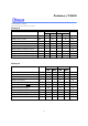
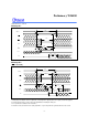
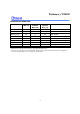
Write Cycle
PARAMETER SYM.
W24100-70L W24100-70LL UNIT
MIN. MAX. MIN. MAX.
Write Cycle Time T
WC
70 - 70 - nS
Chip Selection to End of Write T
CW
50 - 50 - nS
Address Valid to End of Write T
AW
50 - 50 - nS
Address Setup Time T
AS
0 - 0 - nS
Write Pulse Width T
WP
50 - 50 - nS
Write Recovery Time
CS1
, CS2,
WE
T
WR
0 - 0 - nS
Data Valid to End of Write T
DW
30 - 30 - nS
Data Hold from End of Write T
DH
0 - 0 - nS
Write to Output in High Z T
WHZ
* - 25 - 25 nS
Output Disable to Output in High Z T
OHZ
* - 25 - 25 nS
Output Active from End of Write T
OW
5 - 5 - nS
∗
These parameters are sampled but not 100% tested