
Manual


24
U3745BM
4663A–RKE–06/03
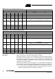
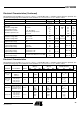
XTO operating frequency
XTO crystal frequency,
appropriate load capacitance must be
connected to XTAL
6.764375 MHz
4.90625 MHz
f
XTO
6.764375
-50 ppm
4.90625
-50 ppm
6.764375
4.90625
6.764375
+50 ppm
4.90625
+50 ppm
MHz
MHz
Series resonance resistor of the
crystal
f
XTO
= 6.764 MHz
4.906 MHz
R
S
150
220
W
W
Static capacitance at Pin XT0 C
XT0
6.5 pF
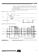
Analog Signal Processing
Input sensitivity ASK 600-kHz IF filter
Input matched according to figure 6
ASK (level of carrier)
BER
£ 10
-3
, B = 600 kHz
f
in
= 433.92 MHz/315 MHz
T = 25
°C, V
S
= 5 V
f
IF
= 1 MHz
P
Ref_ASK
BR_Range0 -106 -110 -113.5 dBm
BR_Range1 -104.5 -108.5 -112 dBm
BR_Range2 -104 -108 -111.5 dBm
BR_Range3 -102 -106 -109.5 dBm
Sensitivity variation ASK for full
operating range including IF filter
compared to T
amb
=25°C, V
S
= 5 V
600-kHz version
f
in
= 433.92 MHz/315 MHz
f
IF
= 0.81 MHz to 1.19 MHz
f
IF
= 0.75 MHz to 1.25 MHz
P
ASK
= P
Ref_ASK
+ DP
Ref
DP
Ref
+3
+5
dB
dB
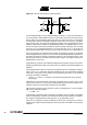
S/N ratio to suppress inband noise
signals
ASK mode
SNR
ASK
11 dB
Dynamic range RSSI ampl. DR
RSSI
60 dB
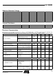
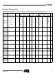
Lower cut-off frequency of the data
filter
CDEM = 33 nF
f
cu_DF
0.11 0.16 0.20 kHz
Recommended CDEM for best
performance
ASK mode
BR_Range0 (Default)
BR_Range1
BR_Range2
BR_Range3
CDEM
39
22
12
8.2
nF
nF
nF
nF
Maximum edge-to-edge time period of
the input data signal for full sensitivity
BR_Range0 (Default)
BR_Range1
BR_Range2
BR_Range3
t
ee_sig
1000
560
320
180
µs
µs
µs
µs
Minimum edge-to-edge time period of
the input data signal for full sensitivity
BR_Range0 (Default)
BR_Range1
BR_Range2
BR_Range3
t
ee_sig
270
156
89
50
µs
µs
µs
µs
Electrical Characteristics (Continued)
All parameters refer to GND, V
S
= 5 V, T
amb
= 25°C, f
0
= 433.92 MHz and f
0
= 315 MHz, unless otherwise specified. The
possible operating range refer to different circuit conditions: V
S
= 4.5 V to 5.5 V, T
amb
= -40°C to +85°C
Parameters Test Conditions Symbol Min. Typ. Max. Unit
f
cu_DF
1
2
p´ 30kW´ CDEM´
---------------------------------------------------------=