
Manual

4
U3742BM
4735A–RKE–11/03
RF Front End The RF front end of the receiver is a heterodyne configuration that converts the input
signal into a 1 MHz IF signal. According to Figure 2 on page 2, the front end consists of
an LNA (low noise amplifier), LO (local oscillator), a mixer and an RF amplifier.
The LO generates the carrier frequency for the mixer via a PLL synthesizer. The XTO
(crystal oscillator) generates the reference frequency f
XTO
. The VCO (voltage-controlled
oscillator) generates the drive voltage frequency f
LO
for the mixer. f
LO
is dependent on
the voltage at pin LF. f
LO
is divided by a factor of 64. The divided frequency is compared
to f
XTO
by the phase frequency detector. The current output of the phase frequency
detector is connected to a passive loop filter and thereby generates the control voltage
V
LF
for the VCO. By means of that configuration, V
LF
is controlled in a way that f
LO
/64 is
equal to f
XTO
. If f
LO
is determined, f
XTO
can be calculated using the following formula:
f
XTO
= f
LO
/64
The XTO is a one-pin oscillator that operates at the series resonance of the quartz crys-
tal. According to Figure 4, the crystal should be connected to GND via the capacitor CL.
The value of that capacitor is recommended by the crystal supplier. The value of CL
should be optimized for the individual board layout to achieve the exact value of f
XTO
and
hereby of f
LO
. When designing the system in terms of receiving bandwidth, the accuracy
of the crystal and the XTO must be considered.
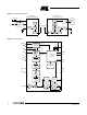
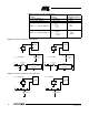
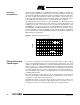
Figure 4. PLL Peripherals
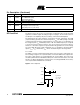
16 MODE
Selecting 433.92 MHz/315 MHz
Low: 4.90625 MHz (USA)
High: 6.76438 (Europe)
17 RSSI Output of the RSSI amplifier
18 TEST Test pin, during operation at GND
19 ENABLE
Enables the polling mode
Low: polling mode off (sleep mode)
High: polling mode on (active mode)
20 DATA Data output/configuration input
Pin Description (Continued)
Pin Symbol Function
DVCC
XTO
LF
LFVCC
LFGND
V
C
C
10
R
1
C
9
S
L
V
S
R
1
= 820 Ω
C
9
= 4.7 nF
C
10
= 1 nF