
Manual

3
U3742BM
4735A–RKE–11/03
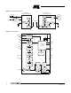
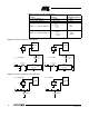
Pin Configuration
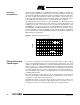
Figure 3. Pinning SO20
1
2
3
4
5
6
7
8
10
9
19
18
17
16
14
15
13
12
11
20
AVCC
AGND
DGND
MIXVCC
LNAGND
LNA_IN
FSK/ASK
CDEM
RSSI
MODE
XTO
LFGND
LF
ENABLE
TEST
NC
LFVCC
DATA
DVCC
SENS
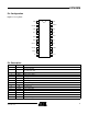
Pin Description
Pin Symbol Function
1 SENS Sensitivity-control resistor
2 FSK/ASK
Selecting FSK/ASK
Low: FSK, High: ASK
3 CDEM Lower cut-off frequency of the data filter
4 AVCC Analog power supply
5 AGND Analog ground
6 DGND Digital ground
7 MIXVCC Power supply mixer
8 LNAGND High-frequency ground LNA and mixer
9LNA_INRF input
10 NC Not connected
11 LFVCC Power supply VCO
12 LF Loop filter
13 LFGND Ground VCO
14 XTO Crystal oscillator
15 DVCC Digital power supply