
Manual

28
U3742BM
4735A–RKE–11/03
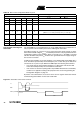
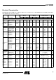
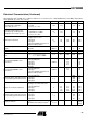
Loop bandwidth of the PLL
For best LO noise
(design parameter)
R
1
= 820 W
C
9
= 4.7 nF
C
10
= 1 nF
B
Loop
100 kHz
Capacitive load at pin LF
The capacitive load at pin LF is limited
if bit check is used. The limitation
therefore also applies to self-polling.
C
LF_tot
10 nF
XTO operating frequency
XTO crystal frequency,
appropriate load capacitance must be
connected to XTAL
6.764375 MHz
4.90625 MHz
f
XTO
6.764375
-30 ppm
4.90625
-30 ppm
6.764375
4.90625
6.764375
+30 ppm
4.90625
+30 ppm
MHz
MHz
Series resonance resistor of the
crystal
f
XTO
= 6.764 MHz
4.906 MHz
R
S
150
220
W
W
Static capacitance of the crystal C
xto
6.5 pF
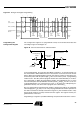
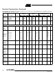
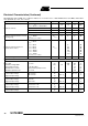
Analog Signal Processing
Input sensitivity ASK
Input matched according to Figure 6
ASK (level of carrier)
BER
£ 10
-3
, f
IF
= 1 MHz
f
in
= 433.92 MHz/315 MHz
T = 25
°C, V
S
= 5 V
P
Ref_ASK
Input sensitivity ASK
BR_Range0 -108 -110 -112 dBm
BR_Range1 -106.5 -108.5 -110.5 dBm
BR_Range2 -106 -108 -110 dBm
BR_Range3 -104 -106 -108 dBm
Sensitivity variation ASK for the full
operating range compared to
T
amb
= 25°C, V
S
=5V
f
in
= 433.92 MHz/315 MHz
f
IF
= 1 MHz
P
ASK
= P
Ref_ASK
+ DP
Ref
DP
Ref
+2.5 -1.5 dB
Sensitivity variation ASK for full
operating range including IF filter
compared to T
amb
=25°C, V
S
= 5 V
f
in
= 433.92 MHz/315 MHz
f
IF
= 0.79 MHz to 1.21 MHz
f
IF
= 0.73 MHz to 1.27 MHz
P
ASK
= P
Ref_ASK
+ DP
Ref
DP
Ref
+5.5
+7.5
-1.5
-1.5
dB
dB
Input sensitivity FSK
Input matched according to Figure 6,
BER
£ 10
-3
, f
IF
= 1 MHz
f
in
= 433.92 MHz/315 MHz
T = 25
°C, V
S
= 5 V
P
Ref_FSK
Input sensitivity FSK
BR_Range0
df
³ ±20 kHz
df
³ ±30 kHz
-95.5
-96.5
-97.5
-98.5
-99.5
-100.5
dBm
dBm
BR_Range1
df
³ ±20 kHz
df
³ ±30 kHz
-94.5
-95.5
-96.5
-97.5
-98.5
-99.5
dBm
dBm
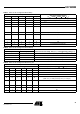
Electrical Characteristics (Continued)
All parameters refer to GND, T
amb
= -40°C to +105°C, V
S
= 4.5 V to 5.5 V, f
0
= 433.92 MHz and f
0
= 315 MHz, unless other-
wise specified. (V
S
= 5 V, T
amb
= 25°C)
Parameters Test Conditions Symbol Min. Typ. Max. Unit