
Manual

27
U3742BM
4735A–RKE–11/03
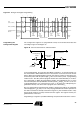
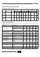
Equivalent
acknowledge
pulse: E_Ack
(Figure 24)
t
8
265 261 128 ´ T
Clk
µs
Equivalent
time window
(Figure 24)
t
9
534 526 258 ´ T
Clk
µs
OFF-bit
programming
window
(Figure 21)
t
10
930 916 449.5 ´ T
Clk
µs
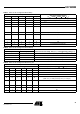
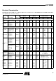
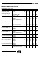
Electrical Characteristics (Continued)
All parameters refer to GND, T
amb
= -40°C to +105°C, V
S
= 4.5 V to 5.5 V, f
0
= 433.92 MHz and f
0
= 315 MHz, unless other-
wise specified. (V
S
= 5 V, T
amb
= 25°C)
Parameter Test Condition Symbol
6.76438 Mhz Oscillator
(Mode 1)
4.90625 Mhz Oscillator
(Mode 0) Variable Oscillator
UnitMin. Typ. Max. Min. Typ. Max. Min. Typ. Max.
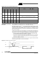
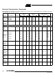
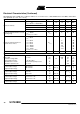
Electrical Characteristics
All parameters refer to GND, T
amb
= -40°C to +105°C, V
S
= 4.5 V to 5.5 V, f
0
= 433.92 MHz and f
0
= 315 MHz, unless other-
wise specified. (V
S
= 5 V, T
amb
= 25°C)
Parameters Test Conditions Symbol Min. Typ. Max. Unit
Current consumption
Sleep mode
(XTO and polling logic active)
IS
off
190 350 µA
IC active
(startup-, bit check-, receiving mode)
pin DATA = H
IS
on
7.0 8.6 mA
LNA Mixer
Third-order intercept point
LNA/mixer/IF amplifier
input matched according to Figure 6
IIP3 -28 dBm
LO spurious emission at RF
In
Input matched according to Figure 6,
required according to I-ETS 300220
IS
LORF
-73 -57 dBm
Noise figure LNA and mixer (DSB) Input matching according to Figure 6 NF 7 dB
LNA_IN input impedance
at 433.92 MHz
at 315 MHz
Zi
LNA_IN
1.0 || 1.56
1.3 || 1.0
kW || pF
k
W || pF
1 dB compression point
(LNA, mixer, IF amplifier)
Input matched according to Figure 6,
referred to RF
in
IP
1db
-40 dBm
Maximum input level
Input matched according to Figure 6,
BER
£ 10
-3
,
ASK mode
P
in_max
-28
-20
dBm
dBm
Local Oscillator
Operating frequency range VCO f
VCO
299 449 MHz
Phase noise VCO/LO
f
osc
= 432.92 MHz
at 1 MHz
at 10 MHz
L (fm) -93
-113
-90
-110
dBC/Hz
dBC/Hz
Spurious of the VCO at ±f
XTO
-55 -47 dBC
VCO gain K
VCO
190 MHz/V