
Manual

3
U3741BM
4662B–RKE–10/04
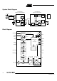
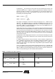
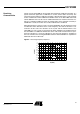
Pin Configuration Figure 1. Pinning SO20
SENS
FSK/ASK
CDEM
AVCC
AGND
DGND
MIXVCC
LNAGND
LNA_IN
NC
DATA
ENABLE
TEST
POUT
MODE
DVCC
XTO
LFGND
LF
LFVCC
1
2
3
4
5
6
7
8
9
10
20
19
18
17
16
15
14
13
12
11
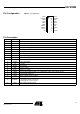
Pin Description
Pin Symbol Function
1 SENS Sensitivity-control resistor
2 FSK/ASK Selecting FSK/ASK. Low: FSK, High: ASK
3 CDEM Lower cut-off frequency data filter
4 AVCC Analog power supply
5 AGND Analog ground
6 DGND Digital ground
7 MIXVCC Power supply mixer
8 LNAGND High-frequency ground LNA and mixer
9LNA_INRF input
10 NC Not connected
11 LFVCC Power supply VCO
12 LF Loop filter
13 LFGND Ground VCO
14 XTO Crystal oscillator
15 DVCC Digital power supply
16 MODE Selecting 433.92 MHz/315 MHz. Low: 4.90625 MHz (USA). High: 6.76438 (Europe)
17 POUT Programmable output port
18 TEST Test pin, during operation at GND
19 ENABLE
Enables the polling mode
Low: polling mode off (sleep mode)
H: polling mode on (active mode)
20 DATA Data output/configuration input