
Manual

25
U3741BM
4662B–RKE–10/04
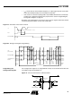
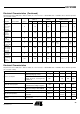
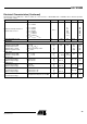
Delay until the
program
window starts
(Figure 17,
Figure 20)
t4 131 129 63.5 × T
Clk
µs
Programming
window
(Figure 17,
Figure 20)
t5 530 522 256 × T
Clk
µs
Time frame
of a bit
(Figure 20)
t6 1060 1044 512 × T
Clk
µs
Programming
pulse (Figure
17, Figure 20)
t7 133 529 131 521
64 ×
T
Clk
256 ×
T
Clk
µs
Equivalent
acknowledge
pulse: E_Ack
(Figure 20)
t8 265 261 128 × T
Clk
µs
Equivalent
time window
(Figure 20)
t9 534 526 258 × T
Clk
µs
OFF-bit
programming
window
(Figure 17)
t10 930 916 449.5 × T
Clk
µs
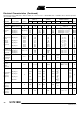
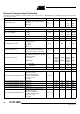
Electrical Characteristics (Continued)
All parameters refer to GND, T
amb
= -40°C to +105°C, V
S
= 4.5 V to 5.5 V, f
0
= 433.92 MHz and f
0
= 315 MHz, unless otherwise specified.
(V
S
= 5 V, T
amb
= 25°C)
Parameter Test Condition Symbol
6.76438-Mhz Osc.
(Mode 1)
4.90625-Mhz Osc.
(Mode 0) Variable Oscillator
UnitMin. Typ. Max. Min. Typ. Max. Min. Typ. Max.
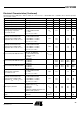
Electrical Characteristics
All parameters refer to GND, T
amb
= -40°C to +105°C, V
S
= 4.5 V to 5.5 V, f
0
= 433.92 MHz and f
0
= 315 MHz, unless otherwise specified.
(V
S
= 5 V, T
amb
= 25°C)
Parameters Test Conditions Symbol Min. Typ. Max. Unit
Current consumption
Sleep mode
(XTO and polling logic active)
IS
off
190 350 µA
IC active
(startup-, bit check-, receiving mode)
pin DATA = H
IS
on
7.0 8.6 mA
LNA Mixer
Third-order intercept point
LNA/mixer/IF amplifier
input matched according to Figure 4
IIP3 -28 dBm
LO spurious emission at RF
In
Input matched according to Figure 4,
required according to I-ETS 300220
IS
LORF
-73 -57 dBm
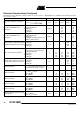
Noise figure LNA and mixer (DSB) Input matching according to Figure 4 NF 7 dB
LNA_IN input impedance
at 433.92 MHz
at 315 MHz
Zi
LNA_IN
1.0 || 1.56
1.3 || 1.0
kΩ || pF
kΩ || pF
1 dB compression point (LNA, mixer, IF
amplifier)
Input matched according to Figure 4,
referred to RF
in
IP
1db
-40 dBm