
Manual

20
U3741BM
4662B–RKE–10/04
Conservation of the Register
Information
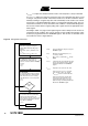
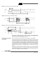
The U3741BM has an integrated power-on reset and brown-out detection circuitry to
provide a mechanism to preserve the RAM register information.
According to Figure 19 on page 21, a power-on reset (POR) is generated if the supply
voltage V
S
drops below the threshold voltage V
ThReset
. The default parameters are pro-
grammed into the configuration registers in that condition. Once V
S
exceeds V
ThReset
,
the POR is canceled after the minimum reset period t
Rst
. A POR is also generated when
the supply voltage of the receiver is turned on.
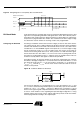
To indicate that condition, the receiver displays a reset marker (RM) at pin DATA after a
reset. The RM is represented by the fixed frequency f
RM
at a 50% duty cycle. RM can be
canceled via an ‘L’ pulse t1 at pin DATA. The RM implies the following characteristics:
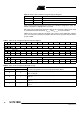
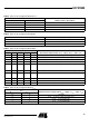
Table 9. Effect of the Configuration Word Lim_min
Lim_min Lower Limit Value for Bit Check
Lim_min < 10 is not applicable (T
Lim_min
= Lim_min × XLim × T
Clk
)
001010 10
001011 11
001100 12
001101 13
001110
14 (Default)
(USA: T
Lim_min
= 228 µs, Europe: T
Lim_min
= 232 µs)
.
.
.
.
.
.
.
.
.
.
.
.
.
.
.
.
.
.
111101 61
111110 62
111111 63
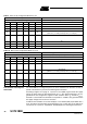
Table 10. Effect of the Configuration Word Lim_max
Lim_max Upper Limit Value for Bit Check
Lim_max < 12 is not applicable (T
Lim_max
= (Lim_max - 1) × XLim × T
Clk
)
001100 12
001101 13
001110 14
.
.
.
.
.
.
.
.
.
.
.
.
.
.
.
.
.
.
011000
24 (Default)
(USA: T
Lim_max
= 375 µs, Europe: T
Lim_max
= 381 µs)
.
.
.
.
.
.
.
.
.
.
.
.
.
.
.
.
.
.
111101 61
111110 62
111111 63