
Manual

14
U3741BM
4662B–RKE–10/04
The bit check limits are determined by means of the formula below:
T
Lim_min
= Lim_min × T
XClk
T
Lim_max
= (Lim_max –1) × T
XClk
Lim_min and Lim_max are defined by a 5-bit word each within the LIMIT register.
Using the above formulas, Lim_min and Lim_max can be determined according to the
required T
Lim_min
, T
Lim_max
and T
XClk
. The time resolution when defining T
Lim_min
and
T
Lim_max
is T
XClk
. The minimum edge-to-edge time t
ee
(t
DATA_L_min
, t
DATA_H_min
) is defined
according to the section “Receiving Mode” on page 15. Due to this, the lower limit
should be set to Lim_min ≥ 10. The maximum value of the upper limit is Lim_max = 63.
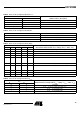
Figure 11, Figure 12 and Figure 13 on page 15 illustrate the bit check for the default bit
check limits Lim_min = 14 and Lim_max = 24. When the IC is enabled, the signal pro-
cessing circuits are enabled during T
Startup
. The output of the ASK/FSK demodulator
(Dem_out) is undefined during that period. When the bit check becomes active, the bit
check counter is clocked with the cycle T
XClk
.
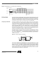
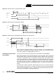
Figure 11 shows how the bit check proceeds if the bit-check counter value CV_Lim is
within the limits defined by Lim_min and Lim_max at the occurrence of a signal edge. In
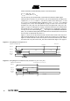
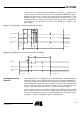
Figure 12, the bit check fails as the value CV_lim is lower than the limit Lim_min. The bit
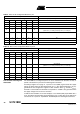
check also fails if CV_Lim reaches Lim_max. This is illustrated in Figure 13 on page 15.
Figure 11. Timing Diagram During Bit Check
Figure 12. Timing Diagram for Failed Bit Check (Condition: CV_Lim < Lim_min)
Bit check
Enable IC
Dem_out
Bit check
Counter
0
234 5
6
245
1
7
81 3 6789 11
12
13 1410
1/2 Bit
15
16 17
18 1
234
56
(Lim_min = 14, Lim_max = 24)
7 8 9 1011121314
15 1 2
34
1/2 Bit 1/2 Bit
Bit check ok
Bit check ok
T
Startup
T
XClk
Bit check
Enable IC
Bit check
Counter
0
2
3
45
6 2451 1 36789
1112
10
1/2 Bit
Startup Mode
0
(Lim_min = 14, Lim_max = 24)
Sleep Mode
Bit check failed ( CV_Lim < Lim_min )
Dem_out
Bit check Mode