
User guide
6
U2745B
4734A–RKE–11/03
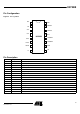
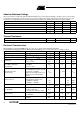
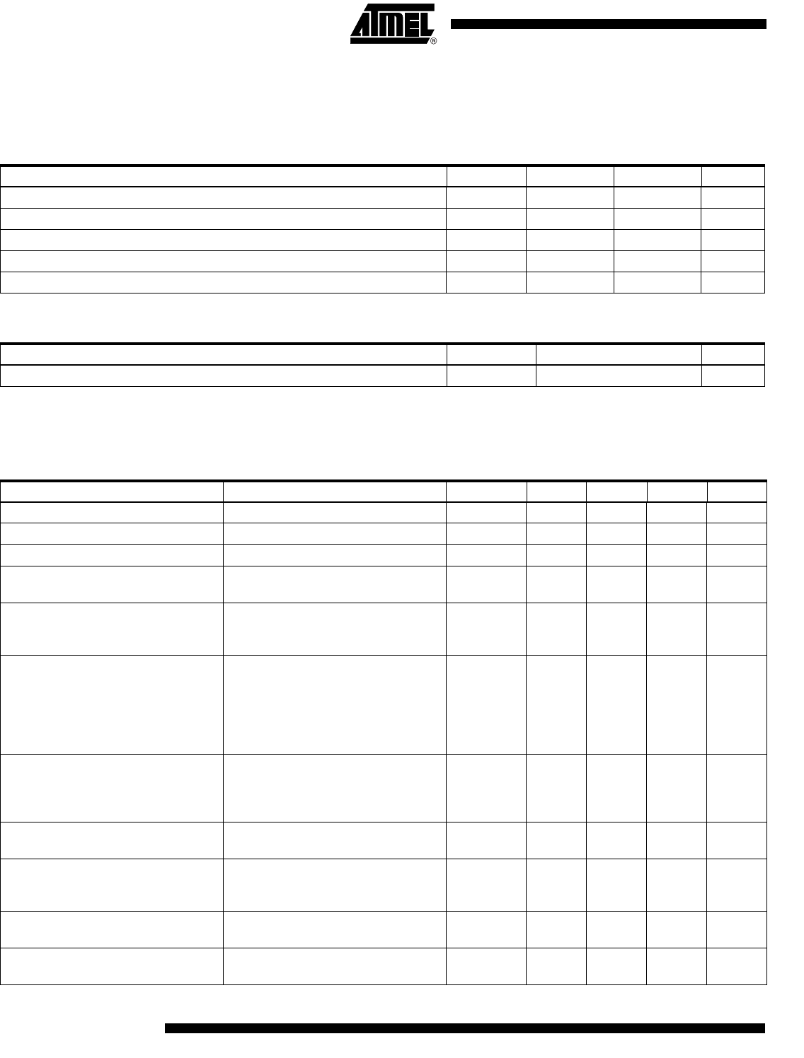
Absolute Maximum Ratings
Stresses beyond those listed under “Absolute Maximum Ratings” may cause permanent damage to the device. This is a stress rating
only and functional operation of the device at these or any other conditions beyond those indicated in the operational sections of this
specification is not implied. Exposure to absolute maximum rating conditions for extended periods may affect device reliability.
Parameters Symbol Min. Max. Unit
Supply voltage V
S
6 V
Power dissipation P
tot
250 mW
Junction temperature T
j
150 °C
Storage temperature T
stg
-55 125 °C
Ambient temperature T
amb
-40 85 °C
Thermal Resistance
Parameters Symbol Value Unit
Junction ambient R
thJA
180 K/W
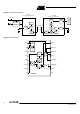
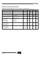
Electrical Characteristics
All parameters are refered to GND (pin 5), V
S
= 3 V, T
amb
= 25°C, unless otherwise specified
The possible operating ranges refer to different circuit conditions: V
S
= 2.2 V to 4.0 V at T
amb
= -40°C to +85°C
Parameters Test Conditions Symbol Min. Typ. Max. Unit
Supply current (power down) V
ASK
, V
FSK
£ 0.3 V, V
S
< 3.6 V IS
off
210µA
Supply current (power up, output OFF) V
ASK
= GND, V
EN
= V
S
, V
S
= 3 V IS
on
4.7 6.2 mA
Supply current (power up, output ON) V
ASK
= V
S
, V
S
= 3 V, R
PWRSET
= 1.2 kW IS
transmit
10 12.5 mA
Output power
V
S
= 3 V, T
amb
= 25°C, f = 433.92 MHz
R
PWRSET
= 1.2 kW P
Ref
135dBm
Output power variation for
f = 315 MHz compared to
f = 433.92 MHz
f = 315 MHz
P
out
= P
Ref
+ DP
Ref
DP
Ref
1.5 dB
Maximum peak output
antenna voltage
at P
out
= 2.0 mW,
the load impedance must be selected
to meet the V
out
maximum
requirement, the supply current is not
dependent on the load impedance
tolerance
V
outmax
V
S
- 0.7 V V
(peak)
Spurious emission
f
o
±(n ´ f
PC
) where f
PC
= 6.78 MHz
Load capacitance at CLK
£ 3pF
f = 230 MHz to 470 MHz
f < 230 MHz, f > 470 MHz
Em
Em
-40
-58
dBC
dBC
Oscillator frequency XTO Crystal frequency = 13.56 MHz f
XTO
13.56 -
30 ppm
13.56
13.56 +
30 ppm
MHz
Loop bandwidth
For best LO noise
Loop filter components:
C
2
= 3.9 nF, C
1
= 15 nF, R
4
= 220 W
B
Loop
100 kHz
Phase noise PLL
Referring to the phase comparator
f
PC
= 6.78 MHz
PN
PLL
-111 -105 dBC/Hz
Phase noise VCO
at 1 MHz
at 36 MHz
PN
VCO
PN
VCO
-90
-122
dBC/Hz